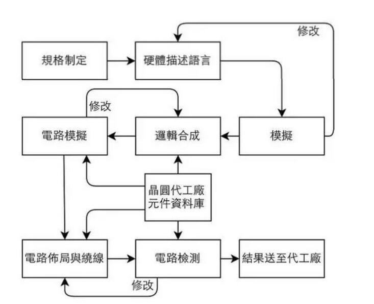
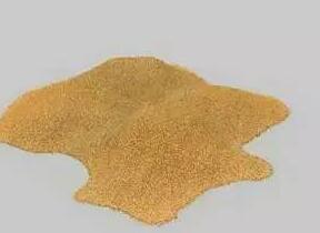
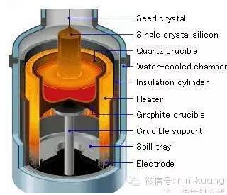
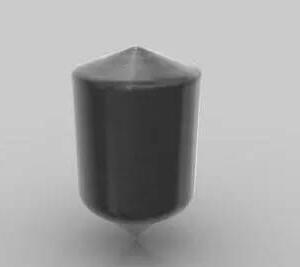
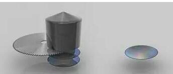
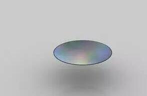
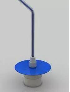
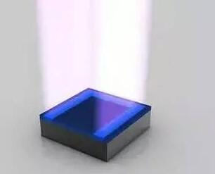
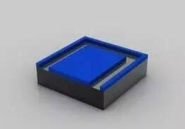
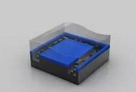
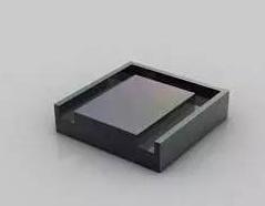
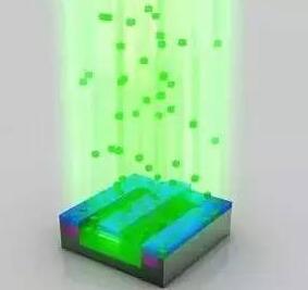
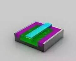
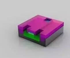
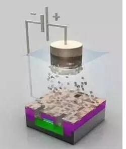
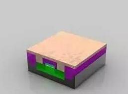
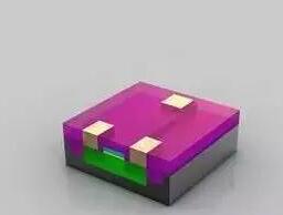
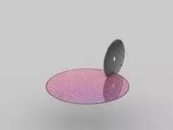
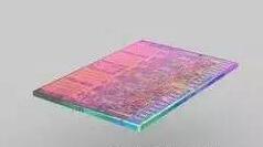
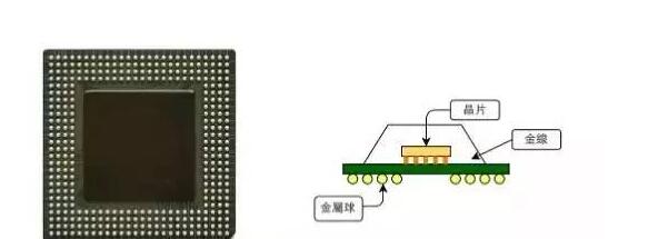
This article mainly explains the T218 semiconductor chip manufacturing, first introduced the T218 semiconductor chip design flow chart, followed by the introduction of the T218 semiconductor chip manufacturing process, and finally introduced the T218 semiconductor chip manufacturing equipment, specifically follow the small series together to find out. Simply put, the chip manufacturing process can be divided into sand raw materials (quartz), silicon ingots, wafers, lithography, etching, ion implantation, metal deposition, metal layers, interconnections, wafer testing and cutting, core packaging, grades Test, packaging and many other steps, and each step contains more detailed processes. 1. Sand: Silicon is the second most abundant element in the earth's crust, and the deoxidized sand (especially quartz) contains up to 25% of silicon, in the form of silicon dioxide (SiO2), which is the basis of the semiconductor manufacturing industry. . 2, silicon smelting: 12 inch / 300 mm wafer level, the same below. The silicon used for semiconductor manufacturing quality, scientifically known as electronic grade silicon (EGS), is obtained by multi-step purification and there is at most only one impurity atom per one million silicon atoms. This figure shows how large crystals are obtained by purifying silicon, and finally the silicon ingot is obtained. 3. Monocrystalline silicon ingots: The overall shape is basically cylindrical with a weight of about 100 kg and a silicon purity of 99.9999%. 4. Ingot cutting: A single silicon wafer that is cut horizontally into a circle, which is also known as Wafer. By the way, why do you know why wafers are round? 5. Wafers: Wafers that have been cut have become virtually flawless after polishing, and surfaces can even be used as mirrors. 6. Photo Resist: The blue part of the picture is the photoresist liquid poured during wafer rotation, similar to the traditional film. Wafer rotation allows the photoresist to be very thin and flat. 7. Photolithography: The photoresist layer is then exposed to ultraviolet light (UV) through the mask and becomes soluble. The chemical reactions that occur during this period resemble changes in the film at the moment the mechanical camera shutter is pressed. A pre-designed circuit pattern is printed on the mask. Ultraviolet light shines on it and forms a circuit pattern for each layer of the microprocessor. This enters the 50-200 nm transistor grade. The transistor is equivalent to a switch and controls the direction of the current. The transistors are now so small that about 30 million can be put on one needle. 8. Dissolving photo-resist: Photo-resist exposed to UV light during the photolithography process is dissolved away, and the patterns and masks left after removal are consistent. 9. Etching: Use chemical substances to dissolve the exposed portions of the wafer, and the rest of the photoresist protects the portions that should not be etched. 10. Remove the photoresist: After the etching is completed, the mission of the photoresist is declared. After the clearance is cleared, the designed circuit pattern can be seen. Photoresist is again wetted with photoresist (blue portion), then photolithographed and the exposed portion washed away. The remaining photoresist is also used to protect the part of the material that is not ion implanted. 11, Ion Implantation (Ion Implantation): In a vacuum system, the ions are irradiated (injected) with ions of accelerated atoms to be doped, thereby forming a special injection layer in the injected region and changing these regions. The conductivity of silicon. After the electric field is accelerated, the injected ion current can exceed 300,000 kilometers per hour. 12. Removing the photoresist: After the ion implantation is completed, the photoresist is also removed, and the implanted region (green portion) is also doped to inject different atoms. Note that the green color at this time is different from before. 13, transistor ready: At this point, the transistor has been basically completed. Three holes were etched in the insulating material (magenta) and filled with copper to interconnect with other transistors. 14. Plating: A layer of copper sulfate is plated on the wafer to deposit copper ions onto the transistor. Copper ions move from the positive (anode) to the negative (cathode). 15. Copper layer: After plating, copper ions are deposited on the wafer surface to form a thin copper layer. 16. Polishing: Polish off excess copper, which is to polish the surface of the wafer. 17, metal layer: transistor grade, a combination of six transistors, about 500 nm. A composite interconnect metal layer is formed between different transistors, and the specific layout depends on the different functionalities required by the respective processor. The surface of the chip looks unusually smooth, but in fact it may contain more than 20 layers of complex circuits. After amplification, it is possible to see an extremely complex circuit network, shaped like a futuristic multi-level freeway system. 18. Wafer test: Core level, approximately 10 mm/0.5 inch. The figure is part of the wafer and is undergoing the first functional test using a reference circuit pattern to compare with each chip. 19. Slicing: wafer level, 300 mm/12 inches. The wafer is cut into blocks, each of which is the core of the chip. The transimpedance amplifier that we can encapsulate is the form of DIE 20. Discard the core: wafer level. The flawed kernel found during the test was abandoned, leaving the preparation ready for the next step 21, package: package level Chip: The most complex product that was made in the cleanest room in the world was actually obtained in hundreds of steps. The previous section of a unit heroes blueprint, said the cleanest working environment, resistance to smog weapon. Recruitment can keep up with the times and admire admiration. Grade test: The last test can identify the key features of each processor, such as the highest frequency, power consumption, heat, etc., and determine the chip's rating. 1, single crystal furnace: German PVA TePla AG, Japan Ferrotec, USA QUANTUM DESIGN 2, gas phase epitaxial furnace: American CVD Equipment Company, American GT Company, French Soitec Company 3, molecular beam epitaxy system: French Riber Company, American Veeco Company, Finland DCA Instruments Company 4, oxidation furnace: British Thermco, Germany Centrotherm thermalsolutions GmbH Co.KG 5, low pressure chemical vapor deposition system: Japan Hitachi International Electric Company 6. Plasma Enhanced Chemical Vapor Deposition System: American Proto Flex Company, Japan Tokki Company, Shimadzu Corporation, Japan 7, magnetron sputtering station: American PVD Company, American Vaportech Company, American AMAT Company 8, chemical mechanical polishing machine: Applied Materials, USA, Nobel Systems, Rtec, USA 9, lithography machine: Asimma (ASML), Pan American Semiconductor, Nikon Japan 10. Reactive ion etching system: Japan's Evatech Corporation, US NANOMASTER Corporation, Singapore REC Corporation 11. ICP plasma etching system: Oxford Instruments UK, Torr America, Gatan, USA 12, ion implantation machine: United States Wiley Semiconductor Equipment Corporation, United States CHA Corporation, United States AMAT Corporation 13, probe test stand: German Ingun company, American QA company, American MicroXact company 14, wafer thinning machine: Japanese DISCO company, German G&N company, Japan OKAMOTO company 15, wafer dicing machine: German OEG company, Japan DISCO company Mini PC Office
Do you know the reason why Mini PC is becoming more and more welcome nowadays? You will realize that Mini PC windows 11 absolutely should be popular if keep thinking deeply a little more, since not only there are all the functions, performance warranty, various ports, but solve the weight problem people struggle when need to move computer in old time. At this shop, you can see Mini PC office, Mini Gaming PC , j4125 Mini PC, etc. Whatever you need for normal office, design drawing, gaming, education learning or teaching, Telecast alive, daily entertainment,etc. You can always find right one here.
Of course, China All In One Business Computer, Education Laptop, Budget Business Laptop, Gaming Laptop , Yoga Laptop , Android Tablet also available at this store, since what we do is customizing Quad Core Laptop, 10.1 android tablet, PC Mini Intel and Business All In One Computer.
Another reason why more and more clients return to us is that quality with competitive price, in time and lifetime after-sales service, customized and multiple service, fast delivery time.
Home Assistant Mini PC,Custom Mini PC,Windows 11 Mini PC,j4125 Mini PC Henan Shuyi Electronics Co., Ltd. , https://www.shuyioemelectronics.com