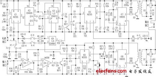
The TGQH9203 obstructive pulmonary rehabilitation device is an electronic device for the treatment of obstructive pneumonia. The device can generate electrical pulses with a wave width of 0.3ms and a continuously adjustable amplitude of 10 to 150V, which has a certain effect on the rehabilitation of obstructive pneumonia. The electrical schematic diagram is now drawn according to the actual object for the reference of users and maintainers. The attached drawing is the schematic diagram of the whole machine. In the figure, IC1, IC2, IC3 and related components constitute the working timing control circuit of the device. Among them, IC1, R1 ~ R3, C1, C2 form a multivibrator, and its output provides a clock signal for IC2. IC3 is a bistable flip-flop composed of 1/2 double D flip-flop CD4013. After the circuit is powered on, the power supply makes the bistable flip-flop enter the stable state of Q = 0 and Q = 1 through C3 and R5. Among them, Q = 0 is directly added to the {11} pin of IC2, so that IC2 starts to count; and Q = 1 causes LED-D to emit light through the resistance RD and switch K-D, indicating that the circuit enters the timing state, and Q = 1 is added to IC9 The {1} foot opens the AND door. IC2 is a fourteen-bit serial counter, and its Q13 and Q14 correspond to frequency division of 2 (13th power) and 2 (14th power), respectively. According to the parameters shown in the figure and the position of switch K1-2, when the circuit works for 60 minutes, Q14 will output a high level, and this level step is added to the CP end of IC3, causing IC3 to flip to Q = 1 and Q = 0 Steady state. Among them, Q = 1 is added to the {11} pin of IC2 to stop IC2 from counting and return to the initial state, and Q = 0 to turn off the LED-D and close the AND door. The integrated dual op amp LM358 forms an input signal conversion circuit, in which IC4-1 is connected as an in-phase linear amplifier, and IC4-2 is connected as a voltage comparator. When the sensor is connected to the input jack, the electrical signal it generates is amplified by IC4-1 and applied to the in-phase input of IC4-2. When the amplitude of the amplified signal exceeds the reference voltage of the comparator, IC4-2 will output a high level and make Q2 saturated and turn on. IC5, IC6 and related components form two pulse-triggered monostable triggers. For IC6, the relevant components are R24 ~ R27, W3 and C11 ~ C15. Normally, the power supply provides 1 / 2EC = 3V voltage to the {2} pin through the R24 and R25 voltage division, and the {4} pin is high, so IC6 maintains the steady state of V0 = 0. The power supply is divided by R22 and R23, so that the collector potential of Q2 is kept at 1 / 2EC, and there is no voltage on capacitor C11. When the external input signal is converted by IC4 to make Q2 saturated, the capacitor voltage at the moment of switching cannot be abruptly changed, so the potential of the {2} pin is nearly grounded. After that, the power supply charges C11 through R24 and Q2, causing IC6 to be negatively charged. The pulse triggers to enter the transient stable state of V0 = 1. At this time, the discharge switch inside IC6 is turned on, and the power is charged to C15 through R27 and W3. After the time of TD1 = 1.1 (R27 + W3) C15, when the voltage on C15 rises above 2 / 3EC, the output flips to V0 = 0, The temporary steady state ends. During the temporary stabilization period, the high level of the IC6 {3} pin output is on the one hand LED-K illuminates, indicating that IC6 has entered the temporary stable state; on the one hand, it is directly applied to the AND gate IC9 to make the {3} pin output high level, Furthermore, Q1 is saturated and turned on. As in the case of IC6, the saturation conduction of Q1 will cause the {2} pin of IC5 to be subjected to a negative pulse, and cause IC5 to enter a transient stable state with a transient steady state duration of TD2 = 1.11R11C8. IC7, IC8 and their related components form two duty-cycle adjustable multivibrators. The start-up of these two oscillators is controlled by the output voltage of IC5 {3} pin. When IC5 enters the transient stable state, the high level output from its {3} pin causes LED-S to emit light through the resistor R5, indicating that IC5 has entered the transient stable state; on the one hand, it is added to the {4} pins of IC7 and IC8. To make IC7 and IC8 oscillate. The oscillating output is taken out by the respective {3} pins, and Q3 and Q4 are excited through R14 and R30, respectively, and a pulse voltage is formed on the primary windings of B1 and B2. The voltage is boosted and added to the output socket to form a composite electrical pulse. W1 and W2 are adjustment potentiometers, and the amplitude of the output electric pulse can be adjusted by changing its value. In summary, the operation of the device can be summarized as: the timing control circuit limits the time of the device's external output, the input conversion circuit provides the trigger condition for IC6, and the high level of IC6 during the temporary stability period is passed through the AND gate and Q1 puts IC5 into a transient stable state, so that IC7 and IC8 can start to vibrate during this period, and output therapeutic electric pulses outward. In the figure, the AN connected between the IC6 {4} pin and ground is a manual button. During the operation of the timing circuit, pressing AN can flip the IC6 {3} pin to a high level, which is passed by IC9 and Q1. Work together; make IC5 enter a temporary stable state, thereby starting IC7 and IC8, so that the treatment electric pulse is manually controlled. Power Meter,Energy Meter, Best power meters,Cycling Power meters,Electrical power meter NINGBO COWELL ELECTRONICS & TECHNOLOGY CO., LTD , https://www.cowellsocket.com