The interconnected architecture in the system has been widely used. Physical constraints such as chip boundaries and board edges require system partitioning. The I/O GPIB or USB, interconnected microprocessor bus, and other standards define the interconnection method. In addition to these standards, connections are also commonly used in asynchronous and peer-to-peer applications. Today, however, the rapid growth of bandwidth between subsystems, the risk of low-latency paths spreading at the subsystem boundaries, and the strict power consumption and cost budgets make everything more complicated. In many designs, it is not possible to populate the system with a CPU bus or a peripheral bus. For subsystems implemented in a system-on-a-chip (SoC), some chip designers can use these subsystems to understand your system interconnect architecture in advance. Due to the low I/O voltage and the very short rise time, point-to-point interconnects encounter significant timing, signal integrity, and board design challenges. For this increasingly complex situation, other solutions are needed. High-speed serial interconnects have been used primarily in the communications industry to transmit data streams over longer distances. Using advanced silicon technology, in many systems, these serial link interfaces become very small, and data rates are high enough that multi-gigabit serial links replace parallel buses and even asynchronous I/O. One obvious example is PCI Express (PCIe). The initial PCI is a very traditional parallel synchronous bus. As the bandwidth requirements of personal computers grew, Intel migrated this topology to multiple lanes of high-speed serial links. Similar developments have also occurred in large-capacity memory devices, and the old AT connection bus has become very familiar with Serial ATA (SATA). The application of these concepts has gone beyond the peripheral bus. To understand why high-speed serial links can be applied to point-to-point connections or even to individual board boundaries, let us understand some system partitioning issues. In an ideal theoretical architecture, system partitioning is entirely a systematic process based on data and control flow graphs. You draw a graph, and then divide the functional modules into subsystems. The subsystems are divided into larger groups. This reduces the bandwidth requirements and increases the latency constraints of the links between the subsystems. You can then implement each connection between the subsystems with the shortest suitable interconnect for the needs of this link. This method is very suitable for blank circuit boards. This is very similar to the early stages of SoC design and FPGA usage. However, most of today's designs begin with commercial chips: application-specific standard products (ASSPs) or microcontroller units (MCUs). These SoCs give us a lot of division requirements, as shown in Figure 1. The chip we choose determines the boundaries of our subsystems and what kind of interconnect technology should be used. If your MCU's only external interconnect is the AMBA APB peripheral bus, or the DDR2 memory bus, and some general purpose I/O pins, then this is your choice. Even so, division is still an important step in system design. Also, you must compare the assumptions made by the SoC designer with the actual physical boundaries of the system, bandwidth requirements, and latency requirements. Therefore, you need to identify subsystems: put together chips that need to exchange large amounts of data, such as SoCs and their DRAMs. It is possible to place chips with narrow bands between them and with low latency requirements in different subsystems such as MCUs and system monitoring analog-to-digital converters (ADCs). After this grouping method includes all the functional modules in the system, it can turn to characterizing the links between subsystems. In an SoC-based system, there seems little point in characterizing the interconnections between subsystems. SoC's I/O options define the interface well. But as a system designer, you still need to answer some important questions. There are still some options that may not be clear. Divide the problem into bandwidth, latency, and cost categories. Bandwidth is the basis of these problems. If your proposed interconnection scheme is feasible, then you should clearly know the bandwidth requirements of each subsystem. In general, this is actually a question of little significance. SoC designers have designed the access path long enough to ensure that the on-chip I/O is much larger than the predicted mission requirements. There is usually enough DRAM bandwidth to handle all the instructions and data streams generated by the chip's CPU cache. There are usually high-speed buses such as PCIe connected to the main system or broadband peripherals and accelerators. Moreover, there is a dedicated I/O interface compatible with the standard. But what if the SoC designer doesn't anticipate what you did? Sometimes, based on your analysis of the system architecture, your choice of SoC fully meets your interface requirements. In other cases, you may find that you encounter bottlenecks in some places, and in some cases you may encounter unused bandwidth or interfaces that are not used at all. In all of these situations, you may rethink the purpose of these interfaces. Or, if you build an SoC by aggregating intellectual property (IP) in the FPGA, you have more flexibility to rearrange the system interconnect architecture. In particular, you should carefully handle the most demanding data flow in your system. It's not a good idea to dump everything on a shared bus, even a fast PCIe bus. If your SoC has multiple DRAM buses, or if you use a single FPGA, one option for these large data streams is to use the DRAM interface as an I/O channel. In an interesting discussion at the most recent DesignCon conference, John Ellis, chief engineer at Synopsys, discussed the possibility of using the new LPDDR3 interface in this way in his article "Promoting the Use of Mobile Memory Beyond Smartphones." Ellis explained that JEDEC specifically designed LPDDR3 for ultra-short-distance broadband connections between smart phone applications SoCs and their main memory, especially for distances up to one centimeter, and optimized the pin layout of SoC and DRAM packages for connection. In this application, the bus can carry very high data rates with relatively low power consumption, even without matching resistors. However, Ellis pointed out that this application is not the only way to use the bus. Ellis said that in the ideal configuration, the bus can operate at 1067 MHz. "Ideal" includes a length of about 1 cm, write leveling and address/control bit de-skew, impedance matching traces, and enough power and ground pins. However, Ellis' simulations show that with reduced frequency, smaller remote termination resistors, and careful routing, the bus can be extended to 8 to 10 cm. Therefore, there are good news and bad news. The good news is that LPDDR3 can be used in various interconnect tasks, not just DRAMs near the SoC. At longer distances, the bus can also be used for links between subsystems. The less good news is that the distance and bandwidth must be considered together, depending on the physical design of the board. For subsystem internal links, the parallel bus frequency and distance trade-off methods bring more serious problems due to the increased bandwidth requirements. At some point, some solutions need to be given. Altera's engineer Kaushik Mittra pointed out that "As the bandwidth increases, at some point you have to give up the parallel bus. The length is also a factor. If a wide bus runs at a very high frequency, at about 40 inches, the trace The timing offset between them accounts for most of the bus cycle time. This does not work at all." We describe this in Figure 2. By using a sufficiently high clock frequency, great attention is paid to impedance matching, trace matching, and power supply methods. In a short chip-to-chip connection, the synchronous parallel bus can achieve a large bandwidth. If the board layout is changed, the same design may fail at a longer distance. The solution is a high-speed serial link. With commercial devices, the single lane operation rate can be as high as 28 Gbps, so several lanes can carry high-speed data streams and be used as high-speed broadband parallel buses. Since each path is independent, its clock is hidden in the data stream, so there is no need to deal with the offset problem, which greatly simplifies the wiring problem. And, as Altera Field Application Engineer Susannah Martin pointed out, even though parallel buses can operate in similar environments, the cost of pins and boards for several serial paths is much lower than for equivalent parallel buses. Fortunately, the high-speed serial interconnect hardware you need has already been provided by the SoC of your choice. Many ASSPs and even some advanced MCUs have 1 Gbps Ethernet (GbE) or 10GbE ports, and in some cases, PCIe ports, all of which can be used in chip-to-chip applications. Even though low-end FPGAs now have generic multi-gigabit transceivers, you can customize these transceivers to meet your link needs. Moreover, Mittra pointed out that some chips include a chip-to-chip serial link that meets the requirements of a particular application environment. One example is Interlaken in a network environment. There are many advantages to carrying wideband data streams between subsystems on a serial link. Martin pointed out that in addition to the above-mentioned low-cost, it can also significantly reduce power consumption. But there is also a problem. Martin suggested that, compared to direct parallel connections, message queuing, serialization, and transmission, and ultimately the process of deserializing and reconstructing messages at the far end, can significantly increase the end-to-end latency. In some systems, it may be necessary to reorganize the logic to solve this delay problem. These problems do not mean that you can only use serial connections between subsystems that are asynchronous to each other. The maximum end-to-end delay of the link is within the overall timing requirements of the system, and you can use the serial link to achieve the transmission between subsystems. You do need to use some reliable methods to resynchronize data at the far end, but this issue is completely different from your use of other clock domain crossover methods. In fact, you can even use the serial link inside the state machine through careful design if needed. This also brings another possibility. So far, we have discussed the use of serial links instead of parallel buses. However, as long as you carefully understand the timing problem, you can also aggregate a set of independent asynchronous I/O pins into a serial link. In fact, some FPGA-based logic simulation systems use this approach to partition logic clouds between two or more internal FPGAs. In the context of vendor-designed ASSPs and MCUs, the scope of the system interconnection architecture seems to have been stipulated. But in fact, as a system designer, you really have a lot of freedom. You can of course choose the chip that you designed. Once you are certain that you are using SoCs, you can reuse the I/Os provided by the chip and use them based on your system's needs, not just the way the chip designer provides them. You can also choose to use programmable logic devices to fully control the interconnect architecture. With this freedom of choice, multi-gigabit serial interconnects will play an increasingly important role as the link bandwidth between subsystems increases. In many cases, SoCs already have transceivers, and of course FPGAs. There are also reliable signal integrity, cost, and power advantages. Using some almost-encapsulated serial link layouts, the final circuit board turns the multilayer board layout problem into a relatively simple design. In some high-performance applications, high-speed serial link I/O has replaced the parallel bus, and future applications will be more extensive. Pin Header section Pin Header section ATKCONN ELECTRONICS CO., LTD , https://www.atkconn.com
System partition 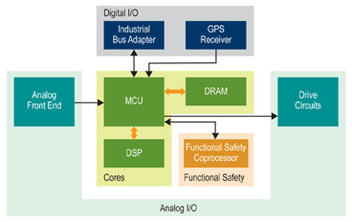
Feature description
Other uses of DRAM bus
Serial selection 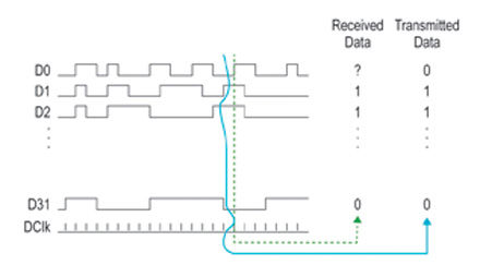
Delay problem
Another solution
Author: Ron Wilson, Altera company
Figure 1. The chips on the motor control board are grouped by subsystem.
Figure 2. Bit-to-bit skew can fail to work properly on a fast parallel bus