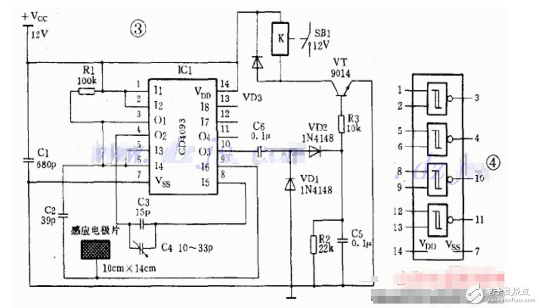
The CD4093 is a model in the CD family of digital integrated circuits fabricated in a CMOS process. There are four Schmitt triggers inside the CD4093, each with a 2-input NAND gate. When a positive or negative polarity signal is input, the flip-flop flips at a different point. The difference between the positive polarity (VP) and negative polarity (VN) voltages is determined by the hysteresis voltage (VH). Today we will first take a look at the cd4093 capacitive inductive control circuit. Figure 3 is a capacitive inductive control circuit fabricated by an integrated circuit The circuit of Figure 3 consists mainly of a four-to-two input NAND gate integrated circuit CD4093 (see Figure 4 for internal circuitry). A NAND gate (1, 2, 3, IC1) of R1, C1 and CD4093 constitutes a 400Hz square wave oscillator, and the square wave of the oscillator output is divided into two paths: one way is directly sent to a NAND circuit (4, 5) , 6 feet, IC2); the other way is sent to a NAND gate (8, 9, 10, IC3) via a capacitor C2. Since IC2 is connected in the form of a NOT gate, its input and output potentials are 180° out of phase, and the signal output from IC2 is coupled to the other input of IC3 via C3 and C4. Since the levels of the two inputs of IC3 are the same. The phase is opposite, so as long as IC1 oscillates normally, at least one of the two inputs of IC3 is at a low level, so the output of IC3 is a stable high level. Due to the action of C6, VT1 is turned off. However, if the input signal of any input of IC3 is canceled or the amplitude of the signal is lowered below the input threshold level of the gate, IC3 outputs a square wave signal. When a conductor approaches the sensing electrode, part of the signal coupled by C2 to the input pin 9 of IC3 is shunted to ground. If the amplitude of the signal after shunting is lower than the threshold level of the NAND gate, IC3 The square wave signal is output. After the signal is rectified by VD1 and VD2, the switching tube VT1 is turned on, and the power of the relay is turned on to make it close. Capacitor C4 is the sensitivity adjustment capacitor. If the circuit needs to work with maximum sensitivity, you can adjust C4 to make the relay just pick up, then adjust C4 to make the relay just disconnect, then seal C4 with high frequency wax or insulating paint. . The components used in the circuit of Figure 3 are common components. Since the CD4093 is a CMOS integrated circuit, it is easily broken by the electrostatic discharge of the soldering iron. Therefore, it is better to solder an integrated circuit socket before the circuit is checked. Plug the CD4093 into the socket. The sensing electrode sheets can be cut with metal cans. We make OBD connector with terminal by ourselves,
soldering type and crimping type are both available. Also 12V and 24V
type. OBD1, OB2, J1939, J1708, J1962, etc. Also molded by different
type, straight type or right-angle type. The OBD connector cables used
for Audi, Honda, Toyota, BWM, etc. We have wide range of materials
source , also we can support customers to make a customized one to
replace the original ones. Sae J1708 Connector,Sae J1939 Connector,OBD2 Diagnostic Connectors,Diagnostic Connector,Deutsch Diagnostic Connector ETOP WIREHARNESS LIMITED , https://www.wireharnessetop.com