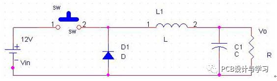
First, the circuit basis of three basic topologies (buck boost buck-boost): 1, the voltage formula of the inductor =, push out ΔI = V × ΔT / L 2, when sw is closed, the inductor energizes voltage VON, when the closing time tON sw is turned off, the inductor voltage VOFF, the off time tOFF 3, the power converter stable operation conditions: ΔION = ΔIOFF, that is, when the inductor is turned on and off, its current changes are equal. Then, from the formula of 1, 2, VON = L × ΔION / ΔtON, VOFF = L × ΔIOFF / ΔtOFF, then the stability condition is volt-second law: VON × tON = VOFF × tOFF 4, period T, frequency f, T = 1 / f, duty ratio D = tON / T = tON / (tON + tOFF) → tON = D / f = TD →tOFF=(1-D)/f Second, the Buck circuit 5. The average input and output current of the capacitor is 0. The average current of the inductor is the average current of the load during the whole period, so there is: IL=Io 6, the diode only flows current when sw is turned off, so ID = IL × (1-D) 7, the average switching current Isw = IL × D 8, known by Kirchhoff's voltage law: When Sw is on: VIN = VON + VO + VSW → VON = VIN - VO - VSW ≈ VIN - VO is assumed to be sufficiently small compared to VSW VO=VIN-VON-VSW≈VIN-VON When Sw is turned off: VOFF = VO + VD → VO = VOFF - VD ≈ VOFF Suppose VD is small enough 9, by 3, 4 can get D = tON / (tON + tOFF) = VOFF / (VOFF + VON) Available from 8: D=VO/{(VIN-VO)+VO} D=VO/ VIN 10, DC current IDC = average inductor current IL, ie IDC≡IL=Io See 5 11, ripple current IAC=ΔI/2=VIN(1-D)D/ 2Lf=VO(1- D)/2Lf From 1, 3, 4, 9, ΔI=VON×tON/L =(VIN-VO)×D/Lf=(VIN-DVIN)×D/Lf=VIN(1- D)xD/ Lf ΔI/ tON=VON/L=(VIN-VO)/L ΔI=VOFF×tOFF/L =VOT(1-D)/L =VO(1-D)/Lf ΔI/ tOFF=VOFF/L=VO/L 12, current ripple rate r = ΔI / IL = 2 IAC / IDC In the critical conduction mode, IAC = IDC, then r = 2 see P51 r=ΔI/ IL=VON×D/Lf IL=(VIN-VO)×D/Lf IL =VOFF×(1-D)/Lf IL=VO×(1-D)/Lf IL 13, peak current IPP = ΔI = 2 IAC = r × IDC = r × IL 14, peak current IPK = IDC + IAC = (1 + r / 2) × IDC = (1 + r / 2) × IL = (1 + r / 2) × IO Determination of the worst input voltage: VO, Io are unchanged, the impact of VIN on IPK: D=VO/ VIN VIN increases ↑→D↓→ΔI↑, IDC=IO, unchanged, so IPK↑. Third, the design case A certain type of DC-DC integrated circuit input voltage range is 4.7-16V, and now there is a circuit used to convert 12V to 3.3V, the maximum output current is 2A. If the switching frequency is 500KHZ, what is the recommended value for the inductor? solution: (1) buck circuit design inductor at VIN=12V (2) Duty cycle: D = VO / VIN = 3.3 / 12 = 0.275 (3) L = VO × (1-D) / rf I = 3.3 * (1 - 0.275) / (0.4 * 500 * 103 * 2) = 5.98 μH (4) IPK=(1+r/2)×IO=(1+0.4/2)*2=2.4A (5) Requires 5.98μH saturation current near 2.4A CBD Vape Pod Shenzhen Xcool Vapor Technology Co.,Ltd , http://www.xcoolvapor.com