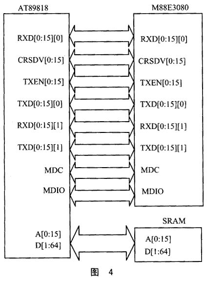
introduction In recent years, network technology has developed rapidly, and Ethernet dominates the market. This design uses Atan's switch chip AT89818 as the core chip, and uses AT89C52 as the system setup and configuration chip. The switch provides great flexibility and manageability for Fast Ethernet upgrades, and it provides 16 multi-channel 10M/100Mbps RJ-45 Ethernet ports. The switch will automatically detect the rate of the device it is connected to, allowing 10Mbps and 100Mbps devices to be used on the same switch without replacing the original network infrastructure. 1 system function The system complies with the IEEE 802.3-802.3u standard and the interface is a 16-port 10/100 Mbps multiplexed switch (using a shielded RJ-45 connector). The system has an address table that can store up to 8K MAC address entries, and has the feature of store-and-forward exchange, which enables it to automatically learn and store addresses in the MAC address table. It has a dynamic O/I buffer of shared memory, thus ensuring Fast and error-free packet storage and packet forwarding; adopts plug-and-play configuration automatic learning mode, supports half-duplex and full-duplex mode, and has an MDI port for cascading. The main technical indicators are Maximum forwarding rate: 14 880 pps/10BASE-T; 148 800 pps/100BASE-TX. Maximum filtration rate: 14 880 pps/10BASE-T; 148 800 pps/100BASE-TX. 2 system composition The switch system adopts AT89818 as the core switch chip; the MCU adopts AT89C52, which is used for control and system setting, and has been connected with the computer; EEPROM uses AT93C46 to store the initialization data required when the switch starts; SRAM uses 64K & TImes; 64 bit W25P243A; PHY0 and PHY1 use 8-port DSP 10/100 PHY; JACK0 and JACK1 are RJ-45 connectors. The system structure is shown in Figure 1. 2.1 AT89818 The AT89818 is the center of the entire hardware system and the core switch chip. The AT89818 can have up to 18 10M/100Mbps multi-switch interfaces. One or several of them can be bundled. The chip has an address table of 8192 MAC address entries. In addition, the VLAN can be set via EEPROM. â—‡ Support store-and-forward function; â—‡ Each VLAN packet can have a 1522B size cache; â—‡ Support aging function and 802.3x flow control; æ— ç¼ Seamlessly connect 64K & TImes; 64-bit or 128K & TImes; 64-bit SRAM; å¹¿æ’ can perform broadcast storm control; â—‡ There are two bundles based on MAC addresses, each group can have 2~6 ports; â—‡ Supports port-based VLAN technology configured via EEPROM; é…ç½® Configurable speed, half-duplex or full-duplex mode, bundle mode, VLAN settings, etc. for each port via EEPROM. The AT89C52 acts as a chip for system setup and control. The MCU can communicate with the computer through the serial port and control and set the management of the switch through the computer. At the same time, it and the AT89818 alternately obtain control of the EEPROM. After the switch chip hands over the control of the EEPROM to the MCU, the MCU reads and writes the EEPROM. After the modification is completed, the MCU can transfer the control right to the switch chip, and the switch chip re-reads the configuration data from the EEPROM. 2.3 Other devices (1) EEPROM With the three-wire CMOS device AT93C46, the data format of the EEPROM can be selected to be 64 &TImes; 16 or 128 × 8 by setting the ORG pin high or low. The CS, SK, DI, and DO are connected to the MCU, and the MCU can read and write data stored in the EEPROM. (2) PHY Use M88E3080. It is an 8-port 10M/100Mbps Fast Ethernet physical layer transceiver with higher signal-to-noise ratio and lower power consumption. It is a product of Marvell Semiconductor Inc. (3) SRAM W25P243A is used. It is a 64K x 64 PIPLINED CMOS high speed static RAM and is a product of Winbond Electronics. 3.1 System clock design Since the clocks of both PHY chips are 50MHz, and the clocks of both SRAM and AT89818 are 75MHz, which is already a high-speed digital circuit design, the signal integrity should be considered in the design. As shown in FIG. 2, the buffer 74LVT244 can increase the driving capability of the clock, and generate two in-phase, extremely small delay and consistent clock outputs to the two PHYs to ensure signal integrity. In addition, the high-speed signal trace should be kept as short as possible in the PCB design to ensure the integrity of the system signal design. 3.2 System design of control between MCU and EEPROM, AT89818 The MCU is connected to the AT93C46 as shown in Figure 3. The MCU can read and write the AT93C46 through EDO, EDI, ESK, and ECS. At the same time, EDO, EDI, ESK, and ECS are also connected to DO, DI, SK, and CS of AT89818. AT89818 and MCU exchange EEPROM control through E2TR. When E2TR is low, AT89818 reads configuration data from EEPROM through DO, DI, SD, CS; when E2TR is high, the four signal lines of AT89818 are in high impedance. State, the control of the EEPROM is handed to the MCU, and the MCU can modify the data in the EEPROM at this time. E2TR must remain low for 30ms after the system is restarted. 3.3 AT89818 is connected to PHY and SRAM The connection between AT89818 and M88E3080 and SRAM is shown in Figure 4. The MDC is a 1 MHz clock output from the switch chip and is used to drive the PHY chip. In order to increase the driving capability, it is considered to first pass the buffer, and MDIO manages the DATA line used by the PHY chip for the switching chip. 4 Application prospects This switch is a network device with fast Ethernet switching, high performance and low power consumption. In recent years, the network has developed rapidly, and many communities are considering fiber-to-the-home when they are building. This equipment can meet the needs of customers with many advantages such as economy, practicality and high efficiency. 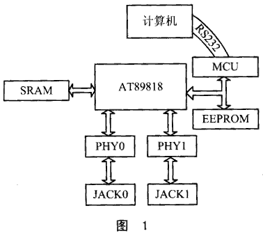
figure 2
2.2 MCU (AT89C52)
image 3
3 system key circuit design