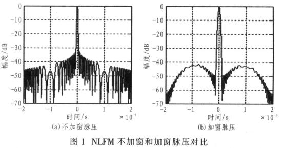
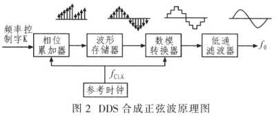
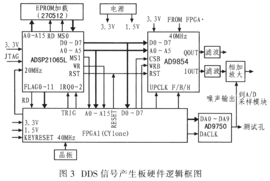
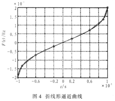
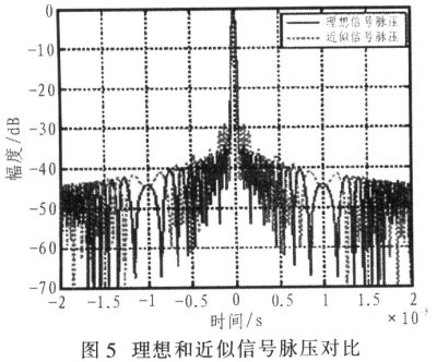
Generation Technology of Nonlinear Frequency Modulation Pulse Compression Radar Signal Based on AD9854 1 Introduction Although the chirp signal has shown significant advantages in improving radar performance, its pulse compression will have higher side lobes, which is not convenient for detection of nearby weak targets. If the method of mismatch windowing is used to suppress the range side lobes, it will cause loss of signal-to-noise ratio and reduce the range resolution of the radar. Non-linear frequency-modulated signals have low side lobe distance, so they can obtain high main side lobe ratio, narrow main lobe width and good Doppler response without weighting. In addition, considering the low intercept probability of radar signals, since the square root of the time-wide bandwidth is inversely proportional to the intercept factor, pulse compression is also one of the main technical measures to achieve low probability of radar interception. Therefore, it is important to study the generation of nonlinear FM signals Practical significance. Adopt the popular DDS device (AD9854), as the main control device, through the piecewise linear broken line approximation method hardware, generate nonlinear frequency modulation signal. 2 Basic principles 2.1 Design of S-type FM function The design of the nonlinear FM function is mainly the design of the S-shaped FM function. The main method of its generation is the waveform design based on various window functions. The commonly used window functions are Hamming, Hanning, and Cosine 4 Square windows, Blackman windows, etc., are designed here using Hamming windows. Using the phase stay principle, the window function of the Hamming window can obtain the group delay of the signal as: In the formula, k is a constant and satisfies Equation (1) finds the inverse function to get the frequency modulation function of the signal f (t) = T-1 (f), so the phase function is: In fact, it is difficult to write the inverse function of equation (1) into an analytical form, but only its numerical inverse function can be obtained, so that the continuous integration of equation (2) becomes numerical integration, so the generation of nonlinear frequency modulation signals is based on numerical methods achieve. Set the parameters of the signal: time width τ = 20μs, bandwidth B = 4 M, sampling frequency fS = 2B, 2 (f) = 0.54 + 0.46cos (2πf / B), and then simulate the signal pulse pressure, figure 1 Given the non-windowed and non-windowed pulse pressure effects of the non-frequency modulated signal, we can see that the non-linear frequency modulated NLFM pulse pressure has good side lobe suppression, and the pulse pressure after windowing is only better than that without windowing Reduced by about 9 dB. 2. 2 DDS principle Figure 2 is the basic principle block diagram of DDS, which is mainly composed of standard reference frequency source, phase accumulator, waveform memory, digital-to-analog converter and so on. Among them, the reference frequency source is a highly stable crystal oscillator, and its output signal is used for the synchronous operation of each component in the DDS. As a frequency synthesizer, DDS applies the sampling principle. That is, the higher reference frequency is used as the sampling clock, and in each cycle of the clock, it is desired to output the sampling value of the frequency waveform. The size of the output sample value is determined by the phase of the phase accumulator output, and the frequency of the output waveform is determined by the frequency control word FTW sent into the DDS. 3 hardware structure design and software implementation 3.1 Introduction to AD9854 The AD9854 digital synthesizer uses advanced DDS technology, and has two internal high-speed, high-performance quadrature D / A converters to implement digitally programmable I and Q synthesizer functions. When the AD9854 is used as an accurate clock source, it can produce sine and cosine outputs with high stability, frequency, phase, and amplitude that are programmable and can be used as a flexible local oscillator for applications in communications, radar, and other fields. The high-speed DDS core of AD9854 provides a frequency resolution of 48 bits (when SYSCLK is 300 MHz, the resolution is adjusted to 1 Hz), and the phase is truncated to 17 bits to ensure a good SFDR. The circuit structure of the AD9854 allows the generation of quadrature output signals with frequencies up to 150 MHz, which can be digitally adjusted at up to 100 MHz / s update frequency. 3. 2 hardware design schemes The signal generation system hardware mainly includes AD9854, ADSP21065L, band-pass filter, FPGA noise generation circuit, DDS output intermediate frequency signal gain control, noise signal addition circuit, and related clock, power supply, FPGA control and other functional units. The DDS module is mainly composed of AD9854, ADSP21065L and corresponding FPGA control logic. ADSP21065L sets the working mode and control word of DDS according to the control timing of FPGA. Figure 3 is a hardware logic block diagram of the signal generation system. Specific module function description: (1) The DDS control module ADSP21065L externally inputs a 20 MHz clock, which operates at a maximum of 60 MHz. It mainly controls the AD9854, writes control words to the AD9854, and interrupts the input IRQ0 to IRQ2 to connect to the FPGA. The external uses pull-up levels. Among them, one is the repetitive periodic signal of the radar, one is the timing signal of the radar waveform, and the other is reserved. Flag0 ~ Flag11 are bidirectional input pins, which mainly generate three control signals for AD9854, and can also be used as external input control signals, requiring external controllability. The external power supply of ADSP-21065L is 3.3 V, which is realized by the on-board (REG1117) DC converter. The loading of ADSP21065L adopts EPROM (27C512) mode and is debugged with JTAG. FPGA uses Cyclone series EP1C3T144, which mainly generates various control signals and timing signals. The output signals of FPGA are: output 1 reset signal to DSP and AD9854, the control signals CS, WR, UPCLK and F / B / H of AD9854. 20 MHz DSP clock signal and 40 MHz AD9854 clock signal. (2) The highest operating frequency of the DDS signal generation module DDS AD9854 is 300 MHz. It mainly receives the control word of ADSP-21065L and generates a pulsed radar waveform. When the external input is 40 MHz, the internal frequency multiplier sets its operating frequency to 200 MHz. Its working voltage is 3.3 V, and it can also be obtained by the external input DC power source through the conversion of two REG1117 DC-DC converters on this board. The AD9854 has 5 programmable working modes. Selecting one mode requires programming mode0, mode1, and mode2 in the control register (parallel address 1FH). The five programmable working modes are: single tone (mode 000); non-inclined rise FSK (mode 001); ramp-up FSK (mode 010); chirp (mode 011); phase encoding (mode 100). For the NLFM signal, the linear frequency modulation broken line approximation is used, as shown in Figure 4. Therefore, the FM area is divided into several segments, each segment is approximated by a different linear FM, that is, the first segment updates the frequency word, and each subsequent segment updates the frequency increment word, and the time increment word can realize the polyline NLFM signal. (3) Power supply module The input power supply of this signal generation module has +5 V and -5 V, and it needs to generate 3.3 V and 1.5 V, which are realized by using 5 REG1117. Among them 1 slice is DSP, 2 slices are AD9854, 2 slices produce 3.3 V and 1.5 V for FPGA respectively. If the remaining I / O devices also need to use 3.3 V, they are shared with the FPGA. 3.3 Software implementation method After determining the time-frequency curve of the linear frequency modulation LFM signal or the nonlinear frequency modulation NLFM signal, according to the form of the signal and the accompanying parameters, set and real-time control DDS and other hardware to generate the required frequency modulation signal. It can be known from the analysis that the AD9854 has a linear frequency modulation generation mode, so only the mode control word, frequency control word, frequency increment word, time increment word of the linear frequency modulation signal need to be set, and the output is stopped at an appropriate time to obtain the desired Time-wide LFM signal. But for NLFM, you need to segment and approximate its FM function to get it. Commonly used methods are stepped approximation and polyline approximation. Under the same sampling interval, the error of polyline approximation is much smaller, because the theoretical analysis based on curve polynomial expansion, the error of polyline approximation is a component of more than the quadratic term, and the error of stepped approximation is more than the first term Ingredients. And for the anti-S-type NLFM signal to be generated, the middle section is close to linear frequency modulation, so only the two ends need to be refined, and the middle section is linearly processed, so that a high-precision NLFM signal is obtained with as few segments as possible , To reduce the update delay caused by frequent updates of DDS control words. Figure 5 is a comparison of ideal signal pulse pressure and approximate signal pulse pressure. 4 Conclusion The experimental results show that the approximate main side-lobe ratio of the signal is only reduced by 5 dB, and the required performance index can be fully achieved. Considering the selection of the device, since the AD9854 is a parallel data operation, its speed is much higher than that of the serial operation, achieving a higher frequency change of the NLFM signal. At the same time, the device has a 48-bit phase accumulator word length and frequency resolution Up to 7.2x10⁻⁷Hz, which is difficult to achieve by traditional frequency synthesis technology. Low Temperature Pressure Sensor Low Temperature Pressure Sensor,Low Pressure Sensor,Low Cost Pressure Sensor,Low Pressure Sensor Transducer Xiaogan Yueneng Electronic Technology Co., Ltd. , https://www.xgsensor.com![]()
![]() FM bandwidth for the signal.
FM bandwidth for the signal. ![]()