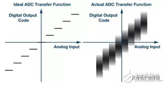
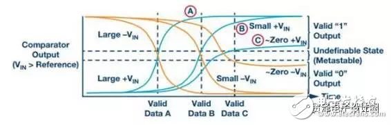
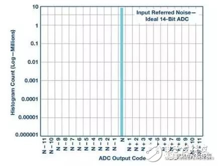
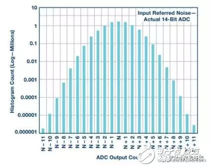
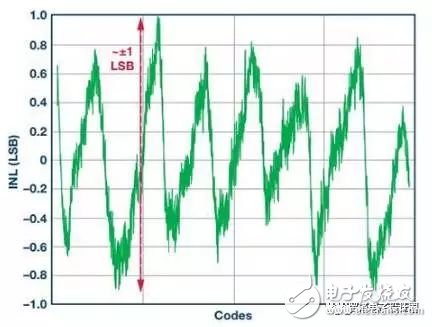
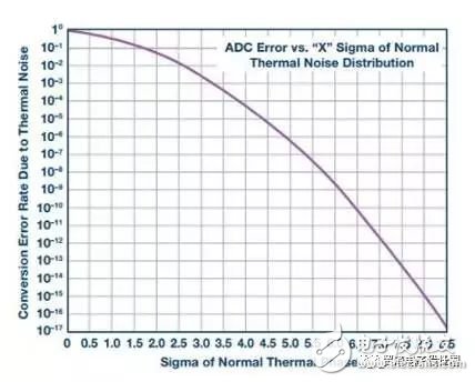
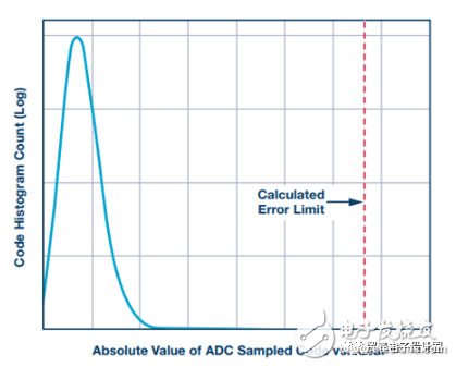
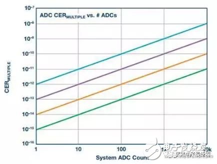
Many high-speed sampling systems, such as electrical test and measurement equipment, life-system health monitoring, radar, and electronic warfare, cannot accept high ADC conversion error rates. These systems look for extremely rare or very small signals over a wide spectrum of noise. False alarms can cause system malfunctions. Therefore, we must be able to quantify the frequency and amplitude of the high-speed ADC conversion error rate. CER and BER First, let's clarify the two major differences in the error rate description. The conversion error rate (CER) is usually the result of incorrect ADC evaluation of analog voltage samples, so the corresponding digital code is not correct compared to the full-scale range of the converter input. The bit error rate (BER) of the ADC can also describe similar errors, but for our discussion, we define the BER as a pure digital reception error; if there is no such error, the converted code data is correct. In this case, the correct ADC digital output is not properly received by downstream logic devices such as FPGAs or ASICs. The extent of the code error and how often it appears is what is discussed in the rest of this article. Simply reading the technical data in the data sheet may make it difficult to grasp the ADC conversion error. Using a single data from the converter's data sheet, of course, you can make some estimate of the conversion error rate, but what exactly is the data quantified? You can't judge how much sample deviation can be considered an error, and you can't determine the test measurement or simulation. Confidence. The definition of "error" must be limited to the amplitude corresponding to the known frequency of occurrence. Error source There are a variety of sources of error that can cause ADC conversion errors, both internal and external. External sources of error include system power glitch, ground bounce, abnormally large clock jitter, and possibly mis-control commands. The recommendations and application notes in the ADC data sheet usually describe the best system layout practices to avoid these external issues. The internal error source of the ADC is primarily attributable to residual processing transfer between the metastable or analog domains, as well as output timing errors in the digital and physical layers. The ADC design team must analyze these challenges during device development. Figure 1. The ideal ADC sample has a single digital output for each bit of the analog resolution at full scale (left). An example of actual ADC output behavior (right) shows some ambiguity associated with internal and external noise. In a set of comparators, a metastable condition can occur when the comparator reference voltage is exactly equal to or very close to the voltage to be compared. The closer the comparison voltage is to the reference voltage, the longer it takes for the comparator to make a full judgment. If the voltage difference between the two is very small or zero, the comparator may not have enough time to finally determine if the comparison voltage is above or below the reference voltage. When the conversion of the sample is complete, the comparator output may be in a metastable third state instead of clearly determining an effective logic output of 1 or 0. This hesitation can affect the entire ADC and can cause conversion errors. Figure 2. The ideal ADC sample has a single digital output for each bit of the analog resolution at full scale (left). An example of actual ADC output behavior (right) shows some ambiguity associated with internal and external noise. In the pipelined ADC architecture, there are other potential sources of conversion error, that is, at the intersection of the interstage boundaries, the residual voltage is transferred from the upper stage to the next stage. For example, if there is an uncorrected gain matching error between the two stages, the transfer of the residual voltage will cause an error in subsequent stages. In addition, glitches responsible for transmitting a voltage to the residual DAC of the next ADC stage may also cause unexpected interference errors in later processing. The thermal noise present in any passive component is the inherent noise component of all ADCs, which determines the absolute noise floor of the ADC processing. In the detailed measurement of the ADC, all of these possible sources of error must be examined and quantified to ensure that the converter is operating without any drops. Noise component The noise that is converted to the input is an inherent component of the ADC conversion defect, including the thermal noise at the input of the ADC. Digital output code histograms with open or floating ADC inputs are often used to quantify them. This noise is usually stated and displayed in the ADC data sheet. The following figure gives an example of this noise amplitude, which is [N] ±11 in this example. Figure 3. When the input is open or floating, the ideal ADC samples and outputs an intermediate level offset code, as shown in the left histogram. The actual ADC will have noise that is converted to the input, which should appear as a Gaussian curved histogram (right side) on a logarithmic scale. The integral nonlinearity (INL) of the ADC is the transfer function of the actual sample code relative to the ideal output over the full-scale input range of the ADC. The ADC data sheet usually also describes this information and gives its curve. The maximum deviation from the ideal code is usually expressed by a certain number of LSBs. Below is an example of an INL curve. Although it reflects a certain amount of absolute error, INL typically has only 0 to 3 codes in most 16-bit or lower resolution high speed ADCs. It is not a major contributor to the actual error rate of the converter. Figure 4. Example of an INL curve, measured on all ADC codes, with a maximum error of ±1 LSB or ±1 code compared to an ideal sample, which is essentially negligible for ADC conversion errors. Test Methods For long-term CER detection, the test method can use a very low ADC input frequency (relative to the clock rate). A straight line is formed between any two adjacent sample points, and the slope of the sine wave can be approximated by the slope of the line. Similarly, input frequencies slightly above the sampling rate are aliased to low frequencies. In this case, there is a predictable and ideal solution that allows each adjacent sample to be within ±1 of the previous code. The input signal frequency and the encoded sample clock frequency must be locked to maintain predictable phase alignment. If this phase is not a constant value, the alignment will be out of phase and the measurement data will be useless. Therefore, in order to calculate the ideal conversion result, the sample (N + 1) – sample(N) should differ by one code, and the amplitude should not exceed one. The sources of predictable small conversion errors inherent to all ADCs include integral nonlinearity, input noise, clock jitter, and quantization noise. All of these noise contributions can be accumulated to obtain the worst limit, and if this limit is exceeded, the error will be considered to come from two adjacent transition samples. The output code number of a 16-bit ADC is 24 or 16 times that of a 12-bit converter. Therefore, this extended resolution affects the number of codes used to limit the conversion error rate test. When everything else is the same, the 16-bit ADC limit will be 16 times wider than the 12-bit ADC. The ADC built-in self-test (BIST) function can be used to determine the error threshold based on thermal noise, clock jitter, and other system nonlinearities. When the error limit is exceeded, the specific sample and its corresponding sample size and error magnitude can be labeled in the ADC core. One of the great benefits of using internal BIST is that it defines the source of the error in the ADC core itself, eliminating the errors caused by receive bit errors that are specific to the digital data transmission output. Once the error threshold is clarified, complete system measurements involving the ADC, the link, and the FPGA or ASIC can be performed to determine the full-component CER. Figure 5. The relationship between the ADC conversion error rate and its thermal noise is usually only obtained through transistor-level circuit simulation. The figure above is an example of a 12-bit ADC. To achieve a 10-15 CER, it must withstand 8 çƒ of thermal noise. Now look at how to calculate the thermal noise contribution: SNR = 20log(VSIGNAL/VNOISE) VNOISE = VSIGNAL × 10^(–SNR/20) To derive the rms noise of the ADC, VFULLSCALE must be adjusted: VNOISE = (VFULLSCALE/(2 × (2) × 10^(–SNR/20) The thermal noise limit of the AD9625 is calculated using the following equation. It is a 12-bit 2.6 GSPS ADC with a design full-scale range (FSR) of 1.1 V and an SNR of 55, 2.508 MHz aliased input frequency. Thermal noise limit = 8 × VINpp × 10 ^ (SNR/20) / 2 √ (2) = 3.39 mV ~ ± 12 codes In this example, for a 10-15 error limit, an 8Σ distribution of thermal noise alone can contribute up to ±12 codes. This should be tested for the ADC's fold-to-input total noise measurement. Note: The equivalent-to-input noise in the data sheet may not be measured based on a sufficiently large sample size (for 10-15 testing). The noise that is converted to the input contains all internal noise sources, including thermal noise. To clarify the boundaries to include as much noise source as possible, including test equipment, we use internal BIST to measure the error magnitude distribution. Using the internal BIST of the AD9625, running at 2.5 GSPS with an aliased AIN frequency of 80 kHz, close to the ADC full scale, CER measurements were performed using nominal power and temperature conditions for a period of 20 days. It is assumed that all ADC processing of analog voltage conversion to digital representation is ideal. Digital data still needs to be accurately transmitted and accurately received in the next stage of processing in the FPGA or ASIC downstream of the signal chain. The level of confusion at this level is usually defined by bit errors or bit error rates. However, the integrated nature of the ADC's data eye diagram output can be measured directly at the end of the PCB trace and compared to the JESD204B receiver eye mask for a good understanding of output quality. When running at 2.6 GSPS in 1 ,, in order to establish a CER of 10-15, the 15th sample of 10 is required to run this test continuously for 4.6 days. For larger flaws, to establish a higher level of confidence, this test needs to run longer. Testing requires a very stable test environment and a clean power supply. If any voltage glitch of the converter's voltage source is not suppressed, it will cause measurement errors and the test will have to start all over again. An FPGA counter can be used to record the difference in amplitude between two adjacent samples exceeding a threshold, and the sample is counted as a conversion error. The counter must accumulate the total number of errors during the entire test period. To ensure that the system's working behavior is as expected, the margin of error and ideal value should also be recorded in the histogram. The time required for testing depends on the sampling rate, the desired test conversion error rate, and the confidence requirements. A CER of less than 10-15 and a 95% confidence level require at least 14 consecutive days of testing. CER can be estimated by extrapolation beyond the measured values, but the confidence is reduced. Measuring the CER of an ADC is a time-consuming process, and you might wonder if you can extrapolate based on known measurements. The good news is that you can do this. However, there are advantages and disadvantages, and readers should keep their eyes open. As we continue to use this method to make a reasonable mathematical estimate of the error rate, the confidence of the estimate will be lower and lower. For example, if the confidence is less than 1%, then knowing the error rate of 10-18 may not be useful. For any given sample, the conversion error threshold may accumulate up to 4 or 5 LSBs. This value may vary slightly depending on ADC resolution, system performance, and application error rate requirements. When this error band is compared to the ideal value, samples that exceed this limit are considered conversion errors. The error band of the ADC can be tested by adjusting the threshold and monitoring typical performance data. The last test limit used is the root mean square of the defect, which is primarily the ADC thermal noise. The test data histogram of the sampled value relative to the ideal value is similar to the discrete Poisson distribution. The main difference between the Poisson distribution and the binomial distribution is that the Poisson distribution has no fixed number of trials. Instead, it uses a fixed time or space interval and records the number of successes in it, similar to the CER test method described above. Any sample recorded that exceeds the error limit calculated from the ideal value is considered a true code error. Figure 6. Using the long-term histogram of the ADC sample compared to the ideal output code, we can detect any deviations beyond the calculated limits. This histogram is similar to the Poisson distribution. system Knowing the CER of a single converter, we can calculate the error rate of an advanced synchronization system with many converters. Many system engineers ask: What is the cumulative ADC conversion error rate in a large, complex system that uses a large number of ADCs? Therefore, for advanced multi-signal acquisition systems, the second consideration is to determine the conversion error rate for a series of (rather than one) converters. At first glance, this seems to be a daunting task. Fortunately, after measuring or calculating the CER of a single ADC, it is not that difficult to extrapolate this error rate to multiple ADCs. In this way, the function becomes a probability expansion equation based on the number of converters used by the system. First, find the probability that a single converter will not have an error. It is only slightly smaller than 1 by 1 minus the error rate value (1–CERSINGLE). Second, how many ADCs are in the system, how many times the probability is multiplied, ie (1–CERSINGLE)#ADCs Finally, by subtracting 1 from the above value, you can get the error rate that the system will go wrong. We get the following equation: CERMULTIPLE =1-(1–CERSINGLE)#ADCs Consider a system that uses 99 ADCs with a single ADC with a CER of 10-15. 1 – CERSINGLE = 0.999****999999CERMULTIPLE = 1 – (0.999****999999) 99= 9.899****99951****00000799095 × 10–14 (~about 10–13) It can be seen that the current CERMULTIPLE value is almost 100 times larger than CERSINGLE (10-15). It can be seen that the conversion error rate of a system with 99 ADCs is roughly equal to the CER of a single ADC multiplied by the number of ADCs in the system. Fundamentally, it is higher than the conversion error rate of a single ADC, limited by the conversion error rate of a single ADC, and by the number of converters used in the system. Therefore, we can conclude that the total conversion error rate is significantly higher for systems with many ADCs than for a single ADC. Figure 7. The CER of a system using multiple converters is proportional to the CER of a single converter multiplied by the number of ADCs. Determining ADC conversion errors can be difficult, but still achievable. The first step is to determine how much conversion error is in the system. A set of appropriate bounded error limits needs to be determined, including a nonlinear benign source of expected ADC operation. Finally, specific measurement algorithms can implement most or all of the tests. Measurement results can be extrapolated beyond the test limits to obtain additional approximations. Connecting Terminals,Micro Connecting Terminal,Aluminum Connecting Terminals,Connecting Copper Terminal Taixing Longyi Terminals Co.,Ltd. , https://www.txlyterminals.com