Introduction to the method flow and practical application of AD analog-to-digital conversion
Let’s take a look at the experimental and product development work that the 51 MCU integrated learning system we will use: water lamps, digital tube display, liquid crystal display, push button switch, buzzer music, relay control, IIC bus, SPI bus, PS/2 experiment, AD analog-to-digital conversion, optocoupler experiment, serial communication, infrared remote control, wireless remote control, temperature sensing, stepper motor control, etc. The main system is shown in Figure 1, and its supporting book tutorial "MCU Quick Start" is shown in Figure 2.
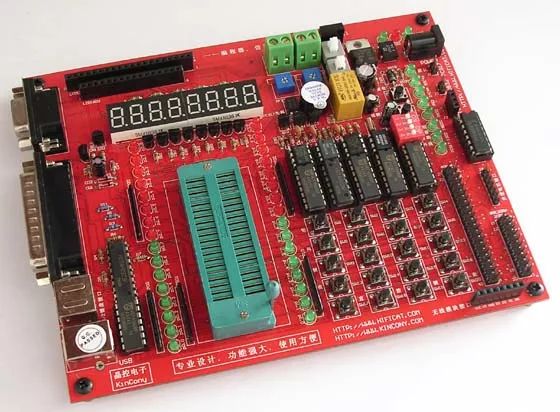
Figure 1 51 MCU integrated learning system host part picture

Figure 2 51 MCU comprehensive learning system supporting book tutorial - "MCU Quick Start"
The above picture shows the hardware platform of the 51 MCU integrated learning system that we will use. As shown in Figure 1, in this experiment we used the integrated system host and the onboard ADC0832 analog-to-digital conversion chip. See the principle and use of other functional modules of the integrated system. Introduction to the previous issues of "Electronic Production" magazine and post-production tutorials.
In industrial control and intelligent instrumentation, real-time control and real-time data processing are usually performed by a microcomputer. The information processed by the computer is always digital, and the relevant parameters that are controlled or measured are often continuously varying analog quantities, such as temperature, speed, pressure, etc., and the corresponding electrical signals are analog signals. Analog storage and processing are difficult and are not suitable for long-distance transmission and are susceptible to interference. In a general industrial application system, the sensor converts the non-electrical analog signal into an analog signal corresponding thereto, and then converts the analog signal into a corresponding digital signal for processing by an analog (Digital) to digital (Digital) conversion circuit. This is a complete signal chain, the analog to digital conversion process is the ADC (Analog to Digital Convert) circuit we often come into contact with.
Introduction to Analog-to-Digital Conversion (ADC)Analog-to-digital conversion principle
The conversion principle of the ADC varies depending on the circuit form of the ADC. The ADC circuit usually consists of two parts: a sample and hold circuit and a quantization and coding circuit. Among them, the quantization and coding circuit is the core component, and any ADC conversion circuit must include such a circuit. There are many forms of ADC circuits, which can usually be combined into two categories: Indirect method: It converts the sample-and-hold analog signal into a time or frequency proportional to the analog quantity, and then converts it into a digital quantity. This is usually done with a clock counter, which is also known as a counter. Its working characteristics are: low working speed, high conversion precision and strong anti-interference ability. Direct method: Converted to digital by comparing the reference voltage with the sample-and-hold signal. Its working characteristics are: high working speed and easy conversion accuracy.
The analog-to-digital conversion process has four phases, namely, sample, hold, quantize, and encode.
Sampling is the process of turning a continuous time signal into a discrete time signal. After sampling, the time-continuous, continuous-value analog signal becomes a time-discrete, numerically continuous signal called a sampled signal. The sampling circuit is equivalent to an analog switch, and the analog switch operates periodically. In theory, the closing time of the analog switch approaches zero in each cycle. At the moment the analog switch is closed (sampling time), we "take" a "sample" of the analog signal.
Quantization is the process of turning a continuous numerical signal into a discrete numerical signal. In theory, after quantization, we can transform time-discrete, numerically continuous sampled signals into time-discrete, numerically discrete digital signals.
We know that in circuits, digital quantities are usually represented in binary code. Therefore, there is an encoding circuit behind the quantization circuit that converts the value of the digital signal into a binary code.
However, quantization and coding always take a certain amount of time to complete, so there is a hold circuit in front of the quantization circuit. Retention is the process of turning a time-discrete, numerically continuous signal into a time-continuous, numerically discrete signal. During quantization and encoding, the hold circuit acts as a constant voltage source that "holds" the signal voltage at the sampling instant at the input of the quantizer. Although the logical keeper is a separate unit, the engineering keeper is always with the sampler. The two are collectively referred to as sample holders.
Introduction to the 8-bit serial A/D converter ADC0832The ADC0832 is an 8-bit resolution, dual-channel A/D converter chip from National Semiconductor. Because of its small size, strong compatibility, and high cost performance, it is well received by MCU enthusiasts and enterprises, and it has a high penetration rate. The ADC083X is a family of serial analog-to-digital converters commonly found on the market. ADC0831, ADC0832, ADC0834, ADC0838 are 8-bit serial I/O analog-to-digital converters with multiplexer switches with high conversion speed (conversion time 32uS), single supply, low power consumption (15mW), suitable for A variety of portable smart meters. This chapter uses ADC0832 as an example to introduce its use.
The ADC0832 is an 8-pin dual in-line dual-channel A/D converter that can perform analog-to-digital conversion on two analog signals, and can be used in single-ended input mode and differential mode. The ADC0832 uses serial communication for channel selection, data acquisition, and data transfer via the DI data input. 8-bit resolution (high resolution up to 256 levels), can adapt to the general analog conversion requirements. The internal power supply input and the reference voltage are multiplexed, so that the analog voltage input of the chip is between 0 and 5V. With dual data output can be used as data verification to reduce data errors, fast conversion speed and strong stability. Independent chip enable inputs make multi-device mounting and processor control more convenient.
The ADC0832 has the following features:
· 8-bit resolution;
· Dual channel A/D conversion;
· Input and output levels are compatible with TTL/CMOS;
· Input voltage is between 0~5V when 5V power supply;
· Operating frequency is 250KHZ, conversion time is 32μS;
· The general power consumption is only 15mW;
· 8P, 14P-DIP (dual in-line), PICC multiple packages;
· Commercial grade chip temperature range is 0 ° C to +70 ° C, industrial grade chip temperature is -40 ° C to +85 ° C;
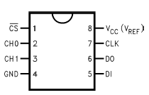
Figure 3 ADC0832 pin diagram
Chip interface description:
· CS_ Chip Select Enable, Low Level Chip Enable.
• CH0 analog input channel 0, or used as IN+/-.
• CH1 analog input channel 1, or used as IN+/-.
· GND chip reference zero potential (ground).
· DI data signal input, select channel control.
· DO data signal output, conversion data output.
· CLK chip clock input.
· Vcc/REF power input and reference voltage input (multiplexed)
How the ADC0832 works:
Under normal circumstances, the interface between ADC0832 and the microcontroller should be 4 data lines, which are CS, CLK, DO, DI. However, since the DO end and the DI end are not used at the same time in communication and the interface with the MCU is bidirectional, DO and DI can be used in parallel on one data line when the I/O port resources are tight. When the ADC0832 is not operating, its CS input should be high. At this time, the chip is disabled, and the levels of CLK and DO/DI can be arbitrary. When performing an A/D conversion, the CS enable must be placed low and held low until the conversion is completely complete. At this point, the chip starts the conversion work, and the processor inputs the clock pulse to the chip clock (CLK) input terminal, and the DO/DI terminal uses the data signal selected by the DI terminal input channel function. The DI terminal must be high before the sinking of a clock pulse, indicating the start signal. Before the second and third pulses sink, the DI terminal should input two bits of data for selecting the channel function.
| Channel address | aisle | Working mode description | ||
| SGL/DIF | ODD/SIGN | 0 | 1 | |
| 0 | 0 | + | - | Differential mode |
| 0 | 1 | - | + | |
| 1 | 0 | + | Single-ended input mode | |
| 1 | 1 | + |
Table 1: Channel Address Settings Table
As shown in Table 1, when the two bits of data are "1" and "0", only CH0 is single-channel converted. When the 2-bit data is "1" or "1", only one channel conversion is performed for CH1. When the two bits of data are "0" and "0", CH0 is input as the positive input terminal IN+, and CH1 is input as the negative input terminal IN-. When the two bits of data are "0" and "1", CH0 is used as the negative input terminal IN-, and CH1 is input as the positive input terminal IN+. After the falling of the third pulse, the input level of the DI terminal loses the input effect, and thereafter the DO/DI terminal starts to use the data output DO to read the converted data. From the falling edge of the 4th pulse, the higher data Bit7 of the conversion data is outputted by the DO terminal, and then the falling edge of each pulse outputs the next bit data. The lowest bit data Data0 is issued until the 11th pulse, and one byte of data output is completed. It is also from this bit that the data of the next opposite byte is output, that is, Data0 is output from the falling edge of the 11th byte. The 8-bit data is then output, and the data output is completed by the 19th pulse, which also marks the end of an A/D conversion. Later, CS is set high to disable the chip, and the converted data can be directly processed. Please refer to Figure 4 for timing description.
When input as a single-channel analog signal, the input voltage of the ADC0832 is 0-5V and the voltage accuracy at 8-bit resolution is 19.53mV, which is (5/256)V. If it is used as an input from the IN+ and IN- inputs, the voltage value is set to a certain larger range, thereby increasing the width of the conversion. However, it is worth noting that when IN+ and IN- are input, if the voltage of IN- is greater than the voltage of IN+, the converted data result is always 00H.
Operating timing of the ADC0832
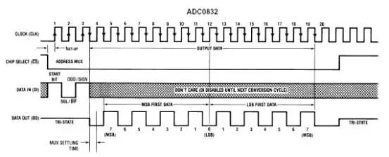
Figure 4 ADC0832 working sequence
ADC0832 software and hardware design exampleAfter learning through the above theory, you should have a certain understanding of analog-to-digital conversion. Then, according to the above instructions, the actual application of ADC0832 will be deepened to deepen the impression. The function of this example is to display the voltage sampled on channel 1 on the LED digital tube, and observe the output reading by changing the input voltage change of channel 1. Before debugging this example, first adjust the function selection switch to the position of ADC0832, as shown in Figure 5 and Figure 6.
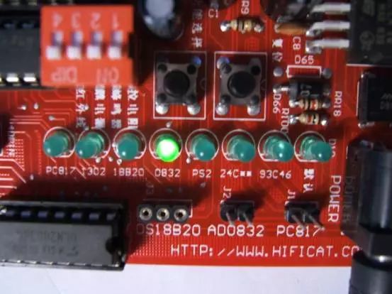
Figure 5 ADC0832 experimental demonstration
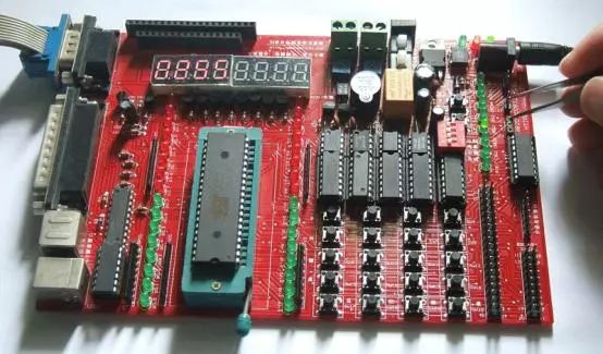
Figure 6 ADC0832 experimental demonstration
Hardware schematic
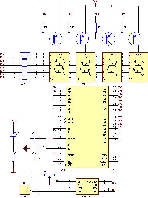
Figure 7 hardware schematic
Program flow chart
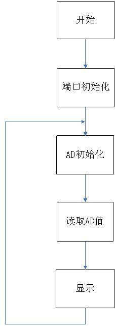
Figure 8 software flow chart
Turntable And Motor For Display And Toy
Turntable and Motor for Display and children toys
Turntable Motor,Toy Display,Record Player Motor
AST Industry Co.,LTD , https://www.astsoundchip.com