Abstract: This paper introduces the principle and implementation scheme of a voice communication terminal module based on AMBE-2000 and DSP chip. The terminal module has many advantages such as simple design, variable speech coding rate, excellent sound quality, high cost performance, low power consumption, and the like, and can be widely applied to satellite communication, short wave, microwave communication and military secret communication. Keywords: vocoder AMBE forward error correction coding (FEC) AMBE-2000 is a single-chip vocoder chip from DVSI (Digital Voice System Inc.). The chip uses an improved multi-band excitation (MBE) algorithm to achieve variable rate low bit rate, high speech quality speech compression coding. Based on AMBE-2000, this paper designs and implements a voice communication terminal module. The module has many advantages such as simple design, variable speech coding rate, excellent sound quality, flexible interface, low operating voltage and low power consumption. It can be widely used in satellite communication, shortwave, microwave communication and secure communication. Practical value. 1 AMBE-2000 Features Overview 1.1 MBE algorithm introduction MBE (Multi-Band Excitation) speech coding technology is a low-rate speech codec technology with high speech quality and strong robustness proposed in the late 1980s. Its improved IMBE algorithm became the speech coding standard for the International Mobile Satellite Organization (INMARSAT) and AUSAT Mobile Satellite Communications. EIA/TIA also selected MBE as the coding standard for North American land mobile communication systems. The MBE speech codec algorithm is widely used in satellite communication, digital voice storage and secure communication due to its superior performance at low rate (<4.8 kbps). The MBE coding method divides the spectrum of one frame of speech into multiple frequency bands in the frequency domain according to the harmonic frequencies of the pitch, and makes clear and voiced (U/V) decisions for each frequency band. For the voiced sound band, the pulse sequence with the pitch as the excitation signal is used as the excitation signal; for the unvoiced band, the white noise is used as the excitation signal. The total excitation signal is composed of the summed excitation signals. The excitation signal is used to excite the channel filter, and finally the speech with higher naturalness is synthesized. The MBE model allows the synthesized speech spectrum to fit well with the original speech spectrum in a fine structure, so the sound quality of the synthesized speech can still maintain a high degree of naturalness at low bit rates. 1.2 AMBE-2000 Features and Features The AMBE-2000 chip is an improved product of the AMBE-1000. Compared with AMBE-1000, its voice compression algorithm is more optimized, the voice quality is higher, and the minimum coding rate is reduced from 2.4kbps to 2.0kbps. In hardware and interface, some improvements have been made and improved. Its efficiency and reliability of compression coding and forward error correction coding (FEC). AMBE-2000 has the following main features: (1) The rate is high and the voice quality is high: there are eight compression rates of 2.0k, 2.4k, 3.6k, 4.0k, 4.8k, 6.4k, 8.0k and 9.6kbps. When the rate is above 4.0 kbps, the voice quality close to long-distance calls can be obtained; when the rate is 2.0 kbps, it still has high intelligibility and naturalness. (2) Variable speed FEC function: The FEC rate can be flexibly selected according to the channel conditions. The rate selection of voice and FEC can be set either by hardware pin or by software. (3) In-chip integrated convolutional encoder and Viterbi decoder. (4) Low power consumption and low complexity. (5) Ability to generate and identify dual tone multi-frequency (DTMF) signals. (6) It has a voice activity detection function, an echo canceling (Echo Cancelling) function, and a comfort noise generating function. (7) The serial channel interface can be set to active and passive modes, and the transmission data can be set to a frame structure or a non-frame structure. The main pin functions of the AMBE-2000 chip are shown in Table 1. The AMBE-2000's operating frequency is recommended to use 16.384MHz, which is connected to the crystal in two ways, as shown in Figure 1 and Figure 2, respectively, is the connection method with active crystal and passive crystal. Pin Both methods can be used, depending on whether the crystal used is active or passive. 2 system hardware design and implementation 2.1 System Block Diagram and Principle 3 is a block diagram of a voice communication terminal module based on AMBE-2000. The communication terminal module is composed of a micro control circuit, an AMBE-2000, a Flash, a timing generation circuit, an A/D, a D/A circuit, and the like. The control circuit adopts TI's TMS320VC5402 eye 2 performance, which is used to control and read and write AMBE-2000, and exchange data with the outside; Flash is a TE28F008 produced by Intel Corporation, which constitutes 1M & TImes; 8bits storage space for storing programs And initialization data; the timing generation circuit is completed by the programmable logic device EPM3032S, which is used to generate various timings required by the system; the A/D and D/A circuits are composed of the TLV320AIC10 and its peripheral circuits. All devices operate at 3.3V. The A/D and D/A chips are connected to the CODEC interface of the AMBE-2000 to exchange PCM data. The AMBE-2000 serial port is connected to the VC5402's multi-channel automatic buffering serial port McBSP (Multichannel Buffered Serial Port) to exchange coded data. The VC5402 is connected to the outside through the HPI (Host Port Interface) port. The data is exchanged through the asynchronous serial port (XF, BIO); the VC5402 and the Flash device use an external parallel 8-bit BOOT method for program loading. As a microcontroller, the TMS320VC5402 is TI's low-power, high-performance fixed-point DSP chip. Its main features include: (1) Fast speed and strong function. (2) With optimized CPU structure, there is 32K bytes of on-chip RAM inside. VC5402 can be used to implement complex DSP algorithms and operations, and can also be used as a microcontroller for intelligent control. (3) Low operating voltage and low power consumption. It can operate at 3.3V or 2.7V and reduces power consumption in low power modes (IDLE1, IDLE2 and IDLE3), making it ideal for wireless mobile devices. (4) Intelligent peripherals. Intelligent peripherals such as multi-channel automatic buffer serial port McBSP and HPI interface for communication with external devices. The McBSP port provides 2K bytes of data buffer read and write capability, which reduces processor overhead. When the instruction cycle is 20ns, the maximum data throughput of McBSP is 50Mbps. Even in IDLE mode, McBSP can work at full speed. In addition to being a microcontroller, the VC5402 can also be used to perform other functions, such as channel coding, encryption, and decryption. It can be flexibly added according to the specific requirements of the system. AMBE-2000 can interface with a variety of A/D and D/A chips. Different A/D and D/A chips are used. The pin CODEC_SEL needs different settings, as shown in Table 2. In this system, the A/D and D/A chips use the TLV320AIC10. TLV320AIC10 is a linear PCM codec chip from TI. The chip has an ADC analog anti-aliasing filter and a digital FIR filter. It has good anti-aliasing and anti-noise capability, programmable input and output gain control, and programmable. ADC and DAC slew rate control, operating voltage is 3.3V ~ 5V, also has a low power mode of operation. The connection between AMBE-2000 and TLV320AIC10 is shown in Figure 4. CODEC_SEL? Eye 1~0? is grounded on the hardware. The A/D mode is set to 16-bit linear PCM. The crystal frequency is 16.384MHz. The frame synchronization clock and the bit synchronization clock are generated by TLV320AIC10 and provided to AMBE-2000. . The programmable logic device EPM3032S is used to generate various other timings required by the system (such as AMBE-2000 channel serial port timing, etc.) and chip select signals. The EPM3032S is a PLD device based on the E2PROM process, and the device scale is about 2000 gates. With ISP (In-System Programmable) capability, it is easy to use. At the time of design, the download interface should be reserved. 3 software programming The working process of the whole system is as follows: After the system is powered on and the TMS320VC5402 is reset, the program and data stored in Flash (28F008) are moved to the internal RAM by the internal self-booting program (BOOT); then the VC5402 resets the AMBE-2000 chip. , start the speech codec. AMBE-2000 completes the encoding and decoding operation of one frame of voice data every 20ms, and exchanges data with VC5402 once. The VC5402 outputs the encoded speech and simultaneously sends the data obtained from the channel or other device to the AMBE-2000 for decoding. The software programming is mainly to program the TMS320VC5402. The program is divided into the main program module, the communication and control module with AMBE-2000, the external data communication module and the BOOT program loading module. Main program module. The module performs program initialization, including initialization of VC5402 interface and registers; reset and rate setting of AMBE-2000, voice activation detection, echo cancellation function setting, initialization of TLV320AIC10, etc. Scheduling control of the service program. The initialization of the TLV320AIC10 is mainly to set its four control registers, in which the control register 1 is used to enable the operational amplifier, enable or bypass the ADC analog anti-aliasing filter, enable or bypass the digital FIR filter, activate Software reset, etc.; the role of control register 2 is low power mode control, frequency division register control (determining the clock frequency and sampling period of the filter); the role of control register 3 is to select the analog signal self-loop and digital signal self-loop, control Continuous data transfer mode, etc.; control register 4 is used to control the input and output gain (by controlling the input and output programmable gain amplifiers). Data exchange between VC5402 and AMBE-2000 is performed in a standard serial manner. The VC5402's McBSP interface can be structurally divided into a data channel and a control channel. The data channel completes the transmission and reception of data; the control channel completes the selection and control of the channel. The interrupt mode is used when writing serial communication subroutines. Each time an interrupt occurs, data transmission and reception are performed once. The VC5402 and the Flash device use an external parallel 8-bit BOOT method for program loading. VC5402 provides a variety of BOOT methods, including: parallel I / O port BOOT, serial port BOOT, HPI port BOOT, external parallel BOOT. These different BOOT methods can meet different application scenarios for users. When writing the BOOT program, you need to set the VC5402 to the microcomputer working mode (MP/MC\ pin low). After the DSP is reset, the program runs the BOOT program from the internal ROM, and the program stored in the Flash device is moved to the internal RAM for execution. 4 system implementation The AMBE-2000's rate setting is in software mode, and the VC5402 sends command word settings through the serial interface. According to the design scheme, when the system sets the voice rate to 2.4 kbps and the FEC is set to 1.2 kbps, the system can work stably in an environment with a channel error rate of 4%, and the system can be conveniently provided as needed. The speech rate and the FEC rate are changed to implement variable rate voice communication. 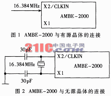
Table 1 AMBE-2000 main pin function Features RATE_SEL[4~0] Used to select the encoding rate and FEC rate CHANN_SEL[1~0] Select channel interface mode (active, passive, frame structure, non-frame structure, etc.) CHAN_RX_DATA,
CHAN_TX_DATA,
CHAN_RX_CLK,
CHAN_TX_CLK,
CHAN_RX_STRB,
CHAN_TX_STRB Serial channel interface pins for channel receive and transmit data, receive clock and transmit clock, receive and transmit frame sync pulses CODEC_SEL[1~0] A/D interface mode selection (such as 16its linear quantization, A rate or μ rate quantization, etc.) CODEC_RX_DATA,
CODEC_TX_DATA,
CODEC_RX_CLK,
CODEC_TX_CLK,
CODEC_RX_STRB,
CODEC_TX_STRB The interface pins with the A/D chip are data reception and data transmission, reception clock and transmission clock, and receiving and transmitting frame synchronization signals. EPR After the chip is reset, this pin has a jump edge, indicating that the first encoded frame is ready, and one frame will be generated after 20ms. ECHOCAN_EN Echo cancellation enable, active high VAD_EN VAD enabled, active high SLEEP_EN Standard sleep mode enabled, active high X2/CLKIN Clock input (16.384MHz) RESETN Reset, active low
Figure 3 Block diagram of the voice communication terminal module based on AMBE-2000
2.2 Hardware Design
Table 2 A/D, D/A type settings A/D, D/A type CODEC_SEL[1~0] Normal 16-bit linear, 8 kHz 00 A/D chip 73311, 32kHz 01 Normal μ rate, 8kHz 10 Ordinary A rate, 8 kHz 11 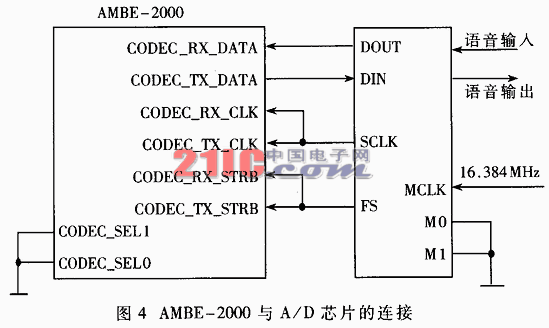
28F008 is Intel's 1M byte flash memory for storing VC5402 programs and initialization data. The connection between 28F008 and VC5402 is shown in Figure 5. In the figure, 28F008 is used as the external data memory of VC5402, the address bus and data bus are connected to the external bus of VC5402, CE is connected to the DS pin of VC5402, R/W pin is connected with MSTRB or connected to WE, OE pin To a jumper, when the jumper is low, the Flash is in the read state. When the jumper is connected high, the flash can be erased or programmable, and the program can be written to the Flash at this time. 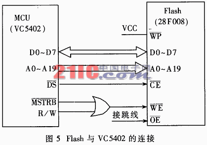
The VC5402 is connected to the outside through the HPI port. The HPI is an 8-bit parallel port, through which the VC5402 can exchange data with external devices. It can be in 8-bit parallel mode or 16-bit parallel mode. The HPI interface mainly implements data movement through three registers, including control registers, data registers and address registers, and the programming is convenient. In addition, as an alternative, data exchange with external devices can also be realized through the asynchronous serial port only through two lines of XF and BIO.