As signal switching speeds in PCBs continue to rise, modern PCB designers must have a deep understanding of and ability to control the impedance of PCB traces. With today's digital circuits operating at shorter signal transmission times and higher clock rates, PCB traces are no longer just simple conductors—they have evolved into transmission lines that require precise design considerations.
In real-world applications, it becomes essential to manage trace impedance when digital signals operate above 1 ns or analog frequencies exceed 300 MHz. One of the most critical parameters for a PCB trace is its characteristic impedance, which is defined as the ratio of voltage to current as a wave propagates along the transmission line. The characteristic impedance of a conductor on a printed circuit board plays a vital role in the overall design, especially in high-frequency circuits. It is crucial to ensure that the trace impedance matches the requirements of the connected devices or signals. This involves two key concepts: impedance control and impedance matching. This article will focus on the challenges of impedance control and stack-up design.
**Impedance Control**
Impedance control refers to the process of maintaining consistent impedance values along signal paths on a PCB. As signal frequencies increase to support faster data transmission, the physical properties of the PCB—such as etching, laminate thickness, trace width, and other factors—can cause variations in impedance, leading to signal distortion. Therefore, in high-speed PCB designs, it is necessary to keep the impedance of the conductive traces within a specific range, known as "impedance control."
The impedance of a PCB trace is influenced by several factors, including the width and thickness of the copper trace, the dielectric constant of the insulating material, the thickness of the dielectric layer, the size of the pad, the ground plane layout, and the surrounding traces. Typical PCB impedance values range from 25 to 120 ohms.
In practice, a PCB transmission line typically consists of a signal trace, one or more reference planes, and an insulating material. The combination of the trace and the reference layers determines the controlled impedance. Multi-layer PCBs allow for various methods of implementing impedance control. However, regardless of the method used, the final impedance value depends on the physical structure of the board and the electrical properties of the materials involved:
- Width and thickness of the signal trace
- Height of the core or pre-preg material on both sides of the trace
- Configuration of the trace relative to the board
- Dielectric constants of the core and pre-preg materials
There are two main types of PCB transmission lines: **microstrip** and **stripline**.
**Microstrip Line**
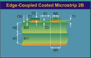
A microstrip line is a single conductor placed above a reference plane, with the top and sides exposed to air (or coated with a protective layer). The reference plane is typically a power or ground plane. In actual PCB manufacturing, a layer of solder mask (often green) is applied to the surface. Therefore, when calculating the impedance of a microstrip line, the model shown below is commonly used.
**Stripline**
A stripline is a conductor sandwiched between two reference planes, as illustrated. The dielectric constants of the materials on either side of the trace (H1 and H2) may differ.
These examples represent only standard forms of microstrip and stripline configurations. There are many variations, such as laminated microstrip lines, which depend on the specific layering structure of the PCB.
Calculating the characteristic impedance of a PCB trace involves complex mathematical equations, often solved using field analysis techniques like boundary element methods. Instead of performing these calculations manually, specialized software like SI9000 is widely used. With this tool, all you need to do is input the relevant parameters, such as:
- Dielectric constant (Er) of the insulating layer
- Trace widths (W1, W2, for trapezoidal shapes)
- Trace thickness (T)
- Thickness of the insulating layer (H)
For clarity, when describing W1 and W2, they are typically treated as equal in most cases. The rule is: W1 = WA, where W is the designed trace width, and A represents the etch loss (refer to the table provided earlier).
The reason for the variation in trace width is due to the etching process during PCB fabrication. As the copper is removed from the top down, the resulting trace has a trapezoidal shape, which affects the final impedance value. Understanding and accounting for this effect is crucial for accurate impedance control in high-speed PCB designs.
Low Voltage Transmission Line
We started to export 10kV Transmission Line Steel Pole to Philippines from 2004 and supply more than 50,000 pcs each year.
Our firm introduced whole set of good-sized numerical control hydraulic
folding equipment(1280/16000) as well as equipped with a series of
good-sized professional equipments of armor plate-flatted machine,
lengthways cut machine, numerical control cut machine, auto-closed up
machine, auto-arc-weld machine, hydraulic redressing straight machine,
etc. The firm produces all sorts of conical, pyramidal, cylindrical
steel poles with production range of dia 50mm-2250mm, thickness
1mm-25mm, once taking shape 16000mm long, and large-scale steel
components. The firm also is equipped with a multicolor-spayed
pipelining. At the meantime, for better service to the clients, our firm
founded a branch com. The Yixing Jinlei Lighting Installation Com,
which offers clients a succession of service from design to manufacture
and fixing.
10kV Steel Pole, Low voltage Steel Power Pole, Steel Power Tubular Pole, Steel Tubular Post
JIANGSU XINJINLEI STEEL INDUSTRY CO.,LTD , https://www.steel-pole.com