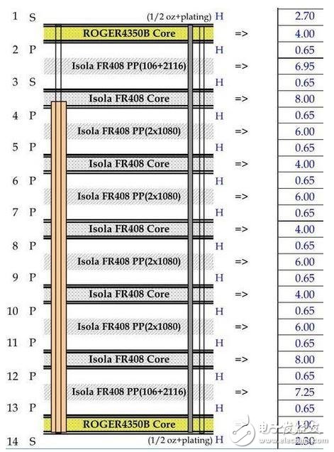
Due to their small size and size, there are few ready-made printed circuit board standards for the growing wearable IoT market. Before these standards came out, we had to rely on the knowledge and manufacturing experience we learned in board-level development and think about how to apply them to unique emerging challenges. There are three areas that we need to pay special attention to: board surface materials, RF/microwave design and RF transmission lines. The PCB typically consists of a laminate which may be fabricated from fiber reinforced epoxy (FR4), polyimide or Rogers materials or other laminates. The insulating material between the different layers is called a prepreg. Wearable devices demand high reliability, so this is a problem when PCB designers are faced with the choice of using FR4 (the most cost-effective PCB manufacturing material) or more advanced and more expensive materials. If wearable PCB applications require high speed, high frequency materials, FR4 may not be the best choice. The dielectric constant (Dk) of FR4 is 4.5, the dielectric constant of the more advanced Rogers 4003 series material is 3.55, and the dielectric constant of the brother series Rogers 4350 is 3.66. Figure 1: Stacked view of a multilayer board showing FR4 material and Rogers 4350 and core layer thickness. The dielectric constant of a stack refers to the ratio of the capacitance or energy between a pair of conductors in the vicinity of the stack to the capacitance or energy between the pair of conductors in the vacuum. At high frequencies, it is preferable to have a small loss, so the dielectric constant is 3. The 66 Roger 4350 is more suitable for higher frequency applications than the FR4 with a dielectric constant of 4.5. Under normal circumstances, the number of PCB layers for wearable devices ranges from 4 to 8 layers. The principle of the layer construction is that if it is an 8-layer PCB, it should be able to provide enough ground and power layers and sandwich the wiring layer. In this way, the ripple effect in crosstalk can be kept to a minimum and electromagnetic interference (EMI) can be significantly reduced. In the board layout phase, the layout scheme generally follows the large formation close to the power distribution layer. This creates a very low ripple effect and the system noise can be reduced to almost zero. This is especially important for the RF subsystem. Compared to Rogers materials, FR4 has a higher dissipation factor (Df), especially at high frequencies. For higher performance FR4 stacks, the Df value is around 0.002, which is an order of magnitude better than normal FR4. However, Rogers' stack is only 0.001 or less. When FR4 materials are used in high frequency applications, there is a significant difference in insertion loss. Insertion loss is defined as the power loss of a signal transmitted from point A to point B when FR4, Rogers, or other materials are used. Msr13 5000Puffs Vape,Disposable Vape 5000 Puffs,Oval E-Cigarette,Vaporizer Pen Guangzhou Yunge Tianhong Electronic Technology Co., Ltd , https://www.e-cigarettesfactory.com