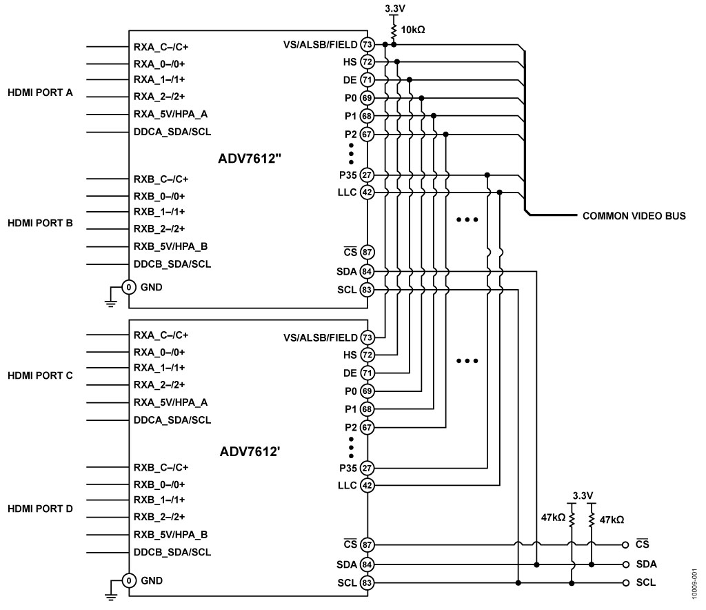
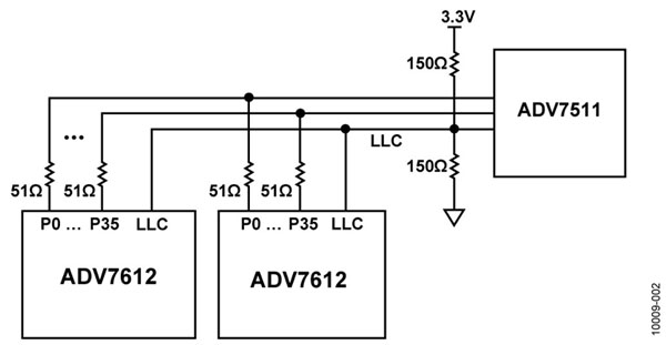
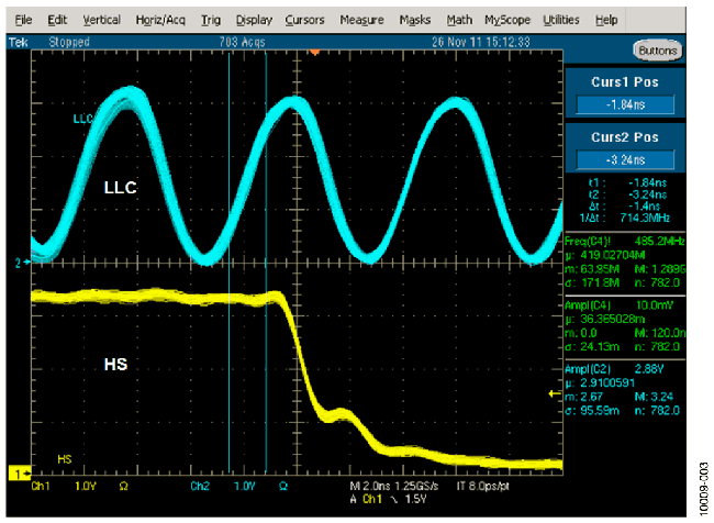
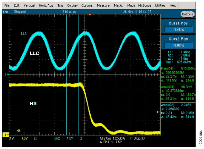
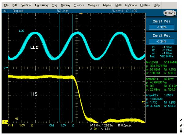
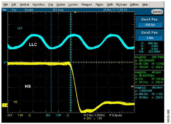
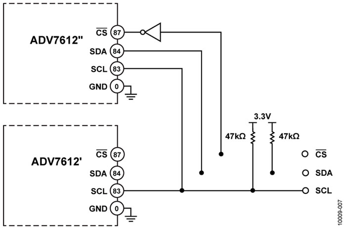
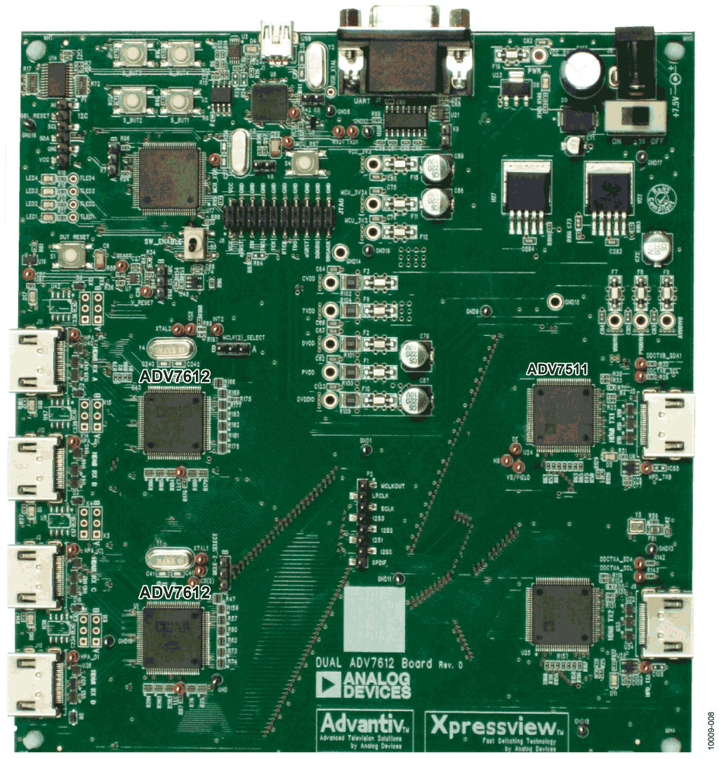
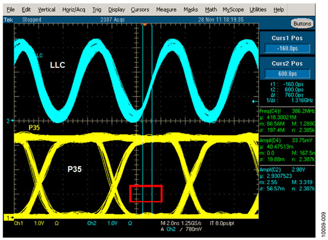
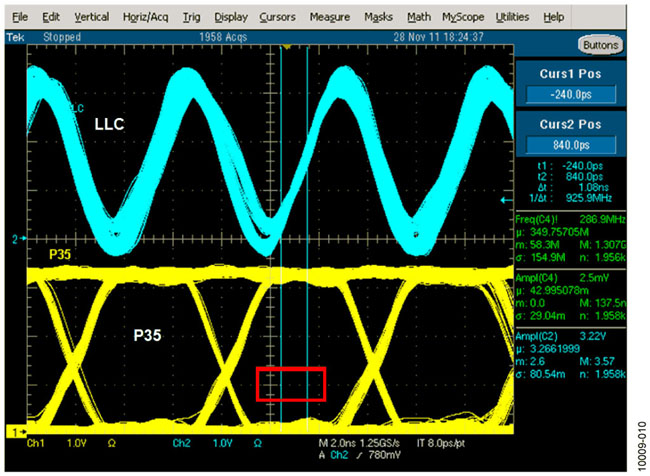
Circuit function and advantage The ADV7612 is a dual-port Xpressview 225 MHz HDMI receiver that enables fast switching between the two inputs. Figure 1 shows the circuit using two ADV7612s as a four-input fast-switching HDMI receiver. This circuit shows the scalability of the ADV7612, up to 225 MHz TMDS (1080p60, 12 bits per channel; 148.5 MHz LLC pixel clock) or UXGA (1600 × 1200, per application) in applications requiring four multiplexed HDMI inputs. Channel 10 bits; 162 MHz LLC pixel clock). This is an economical solution for this application and operates over the extended industrial temperature range of -40°C to +85°C. Figure 1. Dual ADV7612 circuit (simplified schematic: decoupling, termination, reset, and all connections not shown) Circuit description The ADV7612 provides a receive solution for dual HDMI inputs. Figure 1 shows how two ADV7612s can be connected in parallel on a shared video and audio bus to achieve multiplexing of four HDMI inputs. It also shows how to set up I2C communication and how to switch between sources without causing bus collisions. A software package is also provided showing how to handle communication and authentication in an HDMI repeater application (see http://ez.analog.com/community/video). The device must be controlled from the I2C bus in a non-conflicting manner. The board layout of this circuit is critical and should follow the linear principle and use controlled impedance to reduce the risk of reflection and cross-coupling. The complete PCB layout is included in the Design Support package and can be downloaded from: DesignSupport. The ADV7511 HDMI Transmitter is used as a backend device. Bus output status After reset, the ADV7612 tri-states pins P0-P35, HS, VS/FIELD/ALSB, DE, LLC, AP0...AP5, SCLK/INT2, and MCLK/INT2. These pins can be asserted by the registers TRI_PIX, TRI_SYNCS, TRI_LLC, TRI_AUDIO, as described in the UG-216 Hardware User Guide, available at http://ez.analog.com/docs/DOC-1751 Video and audio bus loading Only one ADV7612 can access the AV bus at a time; the second device must remain tri-stated. Assuming the output driver impedance (P0...P35) is 10 Ω to 20 Ω (highest drive strength) and the trace characteristic impedance is 75 Ω, a series resistance of 55 Ω to 65 Ω is required to match the characteristic impedance of the trace. The tri-state output bus driver on the ADV7612 has a maximum capacitance of 20 pF (refer to the electrical specifications in the ADV7612 data sheet). Layout and termination considerations For this design, it must be ensured that the transmission line is properly terminated and has a controlled impedance. Otherwise, reflections (which can occur on longer lines) can adversely affect the data being sent. For pixel lines (P0...P35), video synchronization (VS/FIELD/ALSB, HS, DE) and audio lines (AP0, AP1/I2S_TDM, AP2...AP5, MCLK/INT2, SCLK/INT2)--LLC, it is recommended Use a 51 Ω series termination resistor on the ADV7612 driver side and a 75 Ω trace with a characteristic impedance. Line-locked clock (LLC) lines have the same 75 Ω characteristic impedance and should not have series resistance, but the symmetrical terminations (150 Ω to +3.3 V and 150 Ω to GND) should be used at the far end, as shown in Figure 2. Although the theoretically optimal termination is between 50 Ω and 60 Ω, a symmetrical 75 Ω (2 × 150 Ω) termination was found in the test to increase the swing, centering the signal on the intermediate supply (1.65 V). Very good. The ADV7511 HDMI transmitter is included on the board to transmit the multiplexed outputs of the two ADV7612. Figure 2. Termination of P0...P35 data lines and LLC traces Figures 3 through 6 show various terminated waveforms. In each case, the symmetric LLC termination is placed at the far end (near the ADV7511) and the series termination resistor is placed as close as possible to the two ADV7612 devices, as shown in Figure 2. Measurements were performed on the ADV7511 pin using a Tektronix P6243 FET probe (1 MΩ impedance, 1 GHz bandwidth, capacitance less than 1 pF) and a Tektronix TDS5104B oscilloscope. As can be seen from the waveform, the use of a 2 × 150 Ω termination on the LLC line ensures a maximum swing of 3.3 V. Using 75 Ω on the data line will cause the edge speed to be too low. 33 Ω and 15 Ω on the data line cause a falling edge undershoot (Figures 5 and 6) and a rising edge overshoot (not shown). Therefore, the LLC selects 2 × 150 Ω and the data line uses 51 Ω. The eye diagrams in Figures 9 and 10 are explained. Figure 3. Termination: Symmetrical 2 × 150 Ω on the LLC line and 75 Ω on the data line (HS). Vertical scale: 1 V/div, horizontal scale: 2 ns/div Figure 4. Termination: Symmetrical 2 × 100Ω on the LLC line and 51 Ω on the data line (HS). Vertical scale: 1 V/div, horizontal scale: 2 ns/div Figure 5. Termination: Symmetrical 2 × 68 Ω on the LLC and 33 Ω termination on the data line (HS). Note that 0.5 V is undershoot. Vertical scale: 1 V/div, horizontal scale: 2 ns/div Figure 6. Termination: Symmetrical 2 × 33 Ω on the LLC and 15 Ω termination on the data line (HS). Note that 1 V is undershoot. Vertical scale: 1 V/div, horizontal scale: 2 ns/div Zoom in to I2C access After power-up, both ADV7612 devices will have the same I2C address on the primary map, which can cause collisions. A CS CS pin is provided on both devices, allowing one of two devices to be selected. After the CS line is pulled low, I2C communication is enabled. I2C communication is disabled after the CS line is pulled high. A simple inverter reduces the resources required on the microcontroller side, as shown in Figure 7. Figure 7. I2C access CEC Whether or not CEC is implemented on the board depends on the end user, not on the mandatory. If CEC is not required, the CEC pin should be left floating (as described in Appendix B of UG-216, Recommended Configuration for Unused Pins). This user guide is available for download at http://ez.analog.com/docs/DOC-1751. In the other case, the CEC command should be processed using a standalone engine. XTAL_N, XTAL_P There are two ways to drive the ADV7612 clock. Both devices can have separate crystals connected to the XTAL_N and XTAL_P pins, or they can share the same signal clock. In this circuit, the 1.8 V signal clock from the oscillator is supplied to the pin XTAL_P of both devices. In this configuration, XTAL_N must remain floating. The proper wiring and grounding layout must be ensured to eliminate coupling between sensitive lines. The length of each trace of the bus should be the same. Interrupt Interruptions in both devices must be considered. The ADV7612 has two possible interrupts: INT1 (INT1 pin) and INT2 (provided by SCLK/INT2, MCLK/INT2, or HPA_A/INT2). It is not recommended to use INT2 with pin MCLK/INT2 or SCLK/INT2. Triggering the audio bus through the TRI_AUDIO register will also tristate these pins. Figure 8. Dual ADV7612 Board Solution with ADV7511 Figure 9. Screenshot of the oscilloscope. Figure 10. Screenshot of the oscilloscope. Drive signals from the ADV7612-U1. The LLC line (162 MHz) is measured at the ADV7511 input and pixel line P35. The red rectangle shows the eye mask of the ADV7511. The 2 × 150Ω symmetrical termination on the LLC and the 51 Ω series resistor on the data line. Vertical scale: 1 V/div, horizontal scale: 2 ns/div Drive signal from ADV7612-U43. The LLC line (162 MHz) is measured at the ADV7511 input and pixel line P35. The red rectangle shows the eye mask of the ADV7511. The 2 × 150 Ω symmetrical termination on the LLC and the 51 Ω series resistor on the data line. Vertical scale: 1 V/div, horizontal scale: 2 ns/div
Realpoo Optics offer high quality fused silica laser protective windows are designed for useing with high power fiber lasers, to protective laser optics against damage from material splatter. Laser proteictive window is coated AR coating 1064nm in both sides. The substrate of the window is normally JGS1 or Fused Silica(FS). The diameter 18mm to 55mm is available.
Laser Protective Lens,Laser Cutting Fused Silica,Laser Fused Silica Glass, Laser Protective Window Changchun Realpoo Photoelectric Co., Ltd. , https://www.optics-realpoo.com