Design and Research of Data Acquisition and Control System Based on Single Chip Microcomputer and PC Communication
In the industrial control process, the real-time data of the controlled object needs to be collected, and according to the actual situation of the collected data, real-time monitoring and remote control are performed to complete the corresponding control tasks. In modern industrial control, the accuracy of control and the real-time and stability requirements of control are very high, so there must be a control system that can perform data acquisition, and this system must be able to achieve multi-channel, high precision and Large capacity requirements. From this point of view, the design of data acquisition control system based on single chip and PC communication has very important practical significance.
1. The basic components of the system
1. 1 basic architecture of the system
The basic architecture of the data acquisition and control system based on single chip and PC communication constructed in the paper is shown in Figure 1:
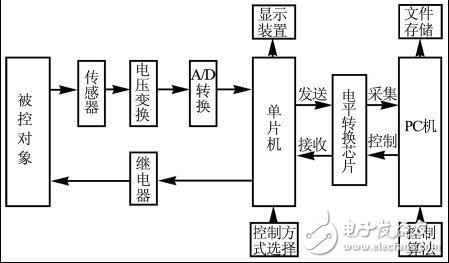
Figure 1 - System basic architecture block diagram
As shown in Figure 1, the controlled object collects the corresponding data through the action of the sensor. After voltage conversion and analog/digital conversion, it is sent to the MCU. The MCU can pass the relay according to the data acquisition situation and the preset program. The specific operation is performed on the controlled object, and the collected data can also be transmitted to the PC through the level conversion chip. The PC can store and process the collected data, and can also improve the control algorithm based on the data, and then send the control signal through the level conversion chip to remotely control the controlled object.
1. 2 system hardware
In this study, there are several very important modules for the hardware composition of the system. The first is the microprocessor module, the RF transceiver module, these two are the core modules, and the other sensor modules, antennas and power management modules are also the focus of the hardware. The chip used in the microprocessor module is the Atmega128L low-power microprocessor. This processor mainly collects data and then processes it, and controls and manages the power consumption and tasks of the entire system. The RF part is effective. The power consumption is controlled, so the energy-saving TI's CC2420 chip is used. This design makes FLASH storage very suitable for low-power products.
The sensor part is selected according to different needs. Each sensor has a unique temperature, pressure and flow sensing system, so for some non-electrical signals, it is necessary to use a sensor to convert it from the voltage conversion module to the entire analog signal.
In the design, the author considered the overall cost and system performance requirements. For the node center design currently used, the Atmega128L MCU was developed. The Atmega128L MCU can perform the data acquisition and processing in a very harsh environment, and it also has a very strong energy-saving capability, the power consumption parameters are the same, must be able to meet the working voltage 1. 8 ~ 3 6V, under the power supply of 2. 2V, can operate stably at 32 kHz operating current at 7 工作 operating current. The connection between the MCU and the PC through the level-shifting chip can work, relying on this way to achieve remote communication. The system designed in this paper can effectively collect various parameter information of the controlled object, and transfer it to the PC terminal to process the corresponding data. At the same time, it can also choose to remotely control the controlled object through the PC.
The system RF signal of this component is transmitted to the CC2420 chip via the antenna. After receiving the relevant signal, the Low Noise Amplifier (LNA) converts it into a 2MHz intermediate frequency, which forms two IF signals of the same direction component and the quadrature component. Subsequently, the two intermediate frequency signals are filtered and amplified, and then converted from analog signals to digital signals. It then performs the selection of the final channel and controls the gain and the like.
In order to ensure that the memory module part can meet the actual needs of the system, it is not possible to rely solely on the Atmega128L internal Flash module, but also to serialize an external flash module, and similarly realize the power-down protection function by means of the module. Specifically, an external flash module can be connected to the Atmega128L via the SPI bus. In the specific work process, the Atmega128L internal storage is the main mode, and the external Flash module AT45DB041B is the slave mode.
The A/D digital-to-analog conversion part adopts the 11-channel 12-bit high-speed TLC2543 conversion chip. The communication between the chip and the single-chip microcomputer is completed by serial communication. Communication can be realized by connecting 4 signal lines. Demand. The four signal lines are the chip select signal CS, the clock signal CLK, the data shift out Dout, and the data shift into Din.
In the display device part of the MCU, the design uses four common-yang digital tubes, which are connected to the segment selection data line and the MCU using a set of I/O ports, and for the bit-selected data lines, they are driven by ULN2003A. The chip is connected to a single set of I/O ports. In the display control section, the digital tube is illuminated one by one by using the cyclic scanning method, and then the high-speed switching is performed, and the visual persistence characteristic of the human body is utilized, so that it appears that the four common digital tubes are stably displayed at the same time.
Road Light,Double Arms Road Light,Off Road Lights,Round Road Light
Yangzhou Heli Photoelectric Co., Ltd. , https://www.heli-eee.com