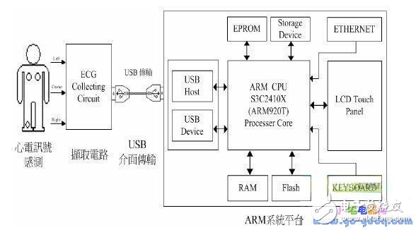
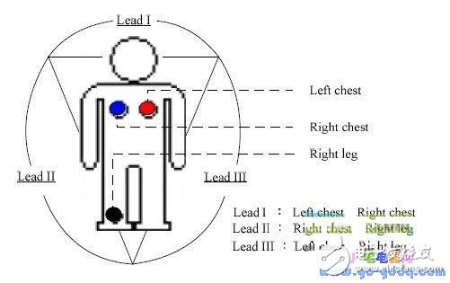
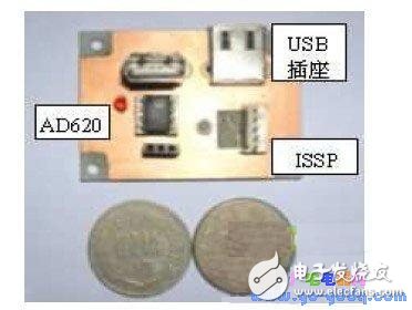
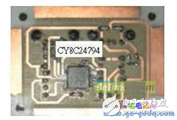
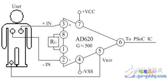
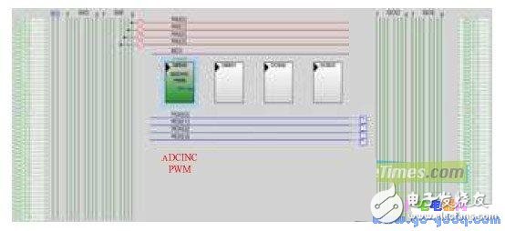
The rapid development of the information industry, the rise of the computer industry, the transmission of information and data is increasingly demanding and rapid, from the earliest contact UART (RS-232), Internet (Ethernet) and other connected transmission development to the present Wireless transmission such as USB transmission (low speed, full speed, high speed), wireless technology (BlueTooth, ZigBee). The scope of the application also summarizes the individual, the family, and the daily life. Electrocardiograms are often used in clinical trials as an important diagnostic tool for measuring heart and lung disease. At present, the data transmission interface of ECG measurement is more commonly used in the RS-232 interface for transmission. The advantages are: (1) The transmission protocol and the transmission packet format are easier to understand. The disadvantages are: (1) the distance to transmit data is limited (2) the transmission speed is slow. However, the emphasis of this paper is on the application of USB interface transmission to transmit ECG signals. The purpose is to use the USB plug-and-play feature to store the ECG signals measured by the user to the storage device of the hardware circuit. The ECG signal can be displayed on the platform's touch panel by connecting to the embedded development platform and mounting the device driver. The user can also carry the ECG waveform to the hospital and let the professional doctor diagnose whether it is abnormal. The system architecture of this thesis consists of ECG signal sensing components (electrode patches), hardware circuits (front-end processing, storage devices), USB interface transmission protocols, system platforms (device driver mounting), System architecture integration and other four major components. The human body uses the electrode patch to extract the weak signal to the hardware circuit of the instrumentation amplifier (AD620) for the first stage amplification, through the programmable system chip PSoC its internal filtering, second-stage amplification, A/D conversion, etc. Converted to USB packet format transmission, the ECG signal is transmitted to the portable mobile platform via the USB interface for signal analysis and display. Its system architecture diagram is shown in Figure 1. Figure 1 system architecture block diagram The main physiological measurement signal of the system architecture is an electrocardiogram (ECG) signal, which can measure the change of the user's cardiac potential activity through the electrocardiographic signal sensing component, and the change is converted into a sensor element through the sensing component. The signal waveform that the researcher can observe, and then the difference in the waveform can be used to know the heart of the subject (for example, heart disease), and the received signal belongs to the analog signal. Electrocardiogram electrode patches (ECG Electrode) are sold on the market. Many of the electrode patches we use are electrode patches produced by KENDALL. The electrocardiogram is mainly to record the change in the projection amount of the heart vector projection to each lead. In this paper, we apply the 3-lead (3-Lead) method to measure and record the ECG waveform we need. Figure 2 shows the placement of the 3-lead electrode patch. Figure 2 Schematic diagram of placement using a 3-lead electrode patch Since the ECG signal sent to the hardware circuit is the DifferenTIal Signal, the way we calculate the ECG signal is: Lead III – Lead II, which is the differential physiology we need. Signal. 3 lead measurement is superior to other lead measurements in sensitivity (difficulty in receiving signals). The emphasis in this paper is on hardware circuits and system platforms, so the measurement is more focused on the ease and convenience of measurement. Portability and small size are topics of heated discussion in the market in recent years. The convenience of plug-and-play USB devices is nothing more than what consumers love. Based on the above point of view, the hardware circuit we designed is easy to carry, and the USB device is used as the transmission interface to achieve the goal of portable USB transmission signals. Figure 3-3-1 shows the entity diagram of the front and back of the hardware circuit. Figure 3-1 Front view of the hardware circuit Figure 3-2 Hardware diagram of the reverse side of the hardware circuit The hardware architecture can be divided into four parts to analyze and explain. The first part is: instrumentation amplifier, the main purpose is to do the first stage amplification of signal processing, and the second part is: programmable system chip PSoC, mainly The purpose of the use is to perform signal filtering, second-stage amplification, A/D conversion, etc. for physiological signal processing. The third part is: USB interface transmission protocol analysis. The purpose and description of the first part of the application of the instrumentation amplifier Since the differential signal generated by the front-end sensing component (electrode patch) is a weak signal, the signal is not easy for the researcher to further analyze and observe, so the AD620 instrumentation amplifier is used to perform about 500 times gain amplification for the weak signal. The output signal is then sent to the programmable system chip PSoC for signal processing. As shown in Figure 4, the user is connected to the instrumentation amplifier. Figure 4 Schematic diagram of the user connected to the instrumentation amplifier Connection instructions: The electrode patch of the user's left chest near the heart should be connected to the instrumentation amplifier PIN 3 (+ IN) as the positive input of the physiological signal source. The symmetrical part of the user's right chest and left patch should be connected to the instrumentation amplifier Pin 2 (-IN) as the physiological signal source negative input. The left foot ground of the user should be connected to Pin 5 (VREF) as the reference ground. The magnitude of the RG resistance can be changed at will, changing its amplification gain. Pins 7 and 4 need to be properly connected to the power supply to drive the instrument to amplify the IC chip. Finally, the output signal is output through Pin 6 to the next stage for signal processing. The second part of the programmable system chip PSoC The waveform is amplified by the instrumentation amplifier to a certain gain. The waveform needs to be filtered to remove noise, second-stage amplification, A/D conversion, data type conversion, etc., before the signal data can be sent to the system platform. Signal processing or storage action. The signal processing summarized by the programmable system chip (PSoC) is: (1) analog signal processing (2) digital signal processing. In the design environment, the analog and digital block modules required by the user can be arbitrarily configured. Figure 5-1 and Figure 5-2 show the configuration of analog and digital block modules. Figure 5-1 Schematic diagram of analog block configuration Car Antenna for Wifi,Car Radio Antenna,Car GPS antenna,FM AM Car antenna Yetnorson Antenna Co., Ltd. , https://www.yetnorson.com