Difference between MEMS technology processing technology and IC technology
Micromachining processes are divided into silicon-based processing and non-silicon-based processing. The following mainly introduces the body processing technology, silicon surface micromachining technology, combined processing, and sequential processing.
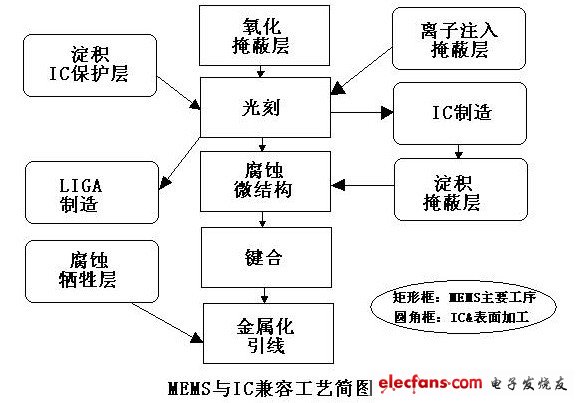
The figure below is a flow chart of the micromachining process.
(1) Body processing technology
Body processing includes processing (corrosion), adhesion processing (coating), modification processing (doping), and bonding processing (bonding).
Mainly introduces corrosion technology.
Corrosion technology mainly includes dry etching and wet etching, and can also be divided into isotropic corrosion and anisotropic corrosion.
(1) Dry etching is the corrosion of a gas using a reactive gas or an ion current. Dry etching can corrode a variety of metals, and can also etch many non-metallic materials; it can be isotropically etched or anisotropically etched, and is commonly used in integrated circuit processes or MEMS processes. According to the etching principle, it can be divided into plasma etching (PE: Plasma Etching), reactive ion etching (RIE: ReacTIon Ion Etching), and inductively coupled plasma etching (ICP: InducTIon Couple Plasma Etching). In plasma gas, isotropic plasma etching is achieved. Directional corrosion can be achieved by ion flow corrosion.
(2) Wet etching is the etching of a corroded silicon wafer into an etching liquid having a determined chemical composition and a fixed temperature. The isotropic corrosion of silicon is equal in the rate of corrosion in the various directions of corrosion of silicon. Such as chemical polishing and so on. The commonly used etching solution is the HF-HNO3 corrosion system, and H2O or CH3COOH is generally added to HF and HNO3. Compared with H2O, CH3COOH can be diluted in a wider range to maintain the oxidation capacity of HNO3, so the oxidizing ability of the etching solution is quite stable during the use period. Anisotropic etching of silicon means having different etching rates for different crystal faces of silicon. For example, the {100}/{111} face has a corrosion rate ratio of 100:1. Based on this corrosion characteristic, various microstructures can be processed on a silicon substrate. Anisotropic etchants generally fall into two categories, one is an organic etchant, including EPW (ethylenediamine, phthalic acid and water) and hydrazine. The other type is an inorganic etchant, including alkaline etching solutions such as KOH, NaOH, LiOH, CsOH and NH4OH.
In the corrosion of the microstructure of silicon, not only the anisotropic etching technique can be used to control the ideal geometry, but also the self-stop technique can be used to control the depth of corrosion. For example, the anode self-stop corrosion, PN junction self-stop corrosion, heterogeneous self-stop corrosion, heavy doping self-stop corrosion, electrodeless self-stop corrosion, and self-stop corrosion by photoelectric effect.
(2) Silicon surface micromachining technology
The Sensor and Actuator team at the University of California, Berkeley, first completed a three-layer polysilicon surface micromachining process and established a system for silicon surface micromachining.
Surface micromachining is the fabrication of a "mechanical" (moving or sensing) portion of a MEMS onto a surface film (such as polysilicon, silicon nitride, etc.) deposited on a silicon crystal, and then partially separated from the silicon portion. The body of sports. The separation mainly relies on the sacrificial layer technology, in which a film which is finally etched (sacrificial) is deposited on a silicon substrate (such as SiO2 can be etched by HF), and then a moving mechanism is deposited thereon. The film is then lithographically fabricated to create a pattern of the mechanism and a channel that etches the underlying film. After all is completed, sacrificial layer etching can be performed to freely release the micro-mechanism.
Silicon surface micromachining techniques include film forming processes and thin film etching processes. The film forming process includes wet film forming and dry film forming. Wet film formation includes electroplating (LIGA process), casting and spin coating, and anodizing. The LIGA process is a method for fabricating an aspect ratio structure by using a light manufacturing process, which uses X-rays emitted from a synchrotron radiation source to irradiate a special PMMA photoresist to obtain an aspect ratio mold, which is then plated or electrolessly plated. The method yields the desired metal structure. Dry film formation mainly includes CVD (Chemical Vapor DeposiTIon) and PVD (Physical Vapor DeposiTIon). The thin film etching process mainly uses wet etching, so it is necessary to select a suitable etching solution.
(3) Combining technology
In the micromachining process, it is sometimes necessary to bond two micromachined substrates to obtain a complicated structure and achieve more functions. The methods for bonding the substrates include soldering, fusion bonding, pressure bonding (solid phase bonding), bonding, anodic bonding, direct silicon bonding, and diffusion bonding.
(four) sequential processing
The sequential processing is a supplement of the simultaneous processing technology, and is often used for processing complex shapes such as molds. The advantage is that it is easy to make a free shape and can be processed for non-planar processing. The disadvantage is that the processing time is long, which is a single piece production and high cost. Including the following:
Sequential removal processing: such as grinding wheel processing for wafer cutting; fine electrical discharge machining, laser beam machining, ion beam machining, STM (scanning tunneling microscope) processing.
Successive adhesion processing: If the ion beam CVD technique is used, only the material of the irradiated portion can be deposited to form a certain structure.
Successive upgrading: For example, the technique of partially modifying the surface of the substrate by means of electron beam or laser irradiation, such as electron beam masking, non-planar lithography, and local doping.
Subsequent bonding processing: such as IC wire bonding, partial bonding, and the like.
The main difference between MEMS and IC technology

Fiber Optic Adapter are used in fiber optic connection, the typical use is to provide a cable to cable fiber connection. People sometimes also name them to be mating sleeves and hybrid adaptors, mating sleeves means this fiber optic adapter is used to connect the same type fiber optic connectors, while hybrid adaptors are the fiber optic adaptor types used to connect different kinds of fiber optic connectors. YLTelecom`s fiber adapter provide reliable solution for fiber connections, single mode fiber optic adaptors and multimode fiber optic adaptors available on request. We adopt high quality raw materials and make these fiber optic adapters strictly according to international standard, this makes our fiber optic adaptors with high performance.
Fiber Optic Adapters FC, SC, ST, LC, MT-RJ, MU, E2000, FC/APC, SC/APC, LC/APC, E2000/APC, Simplex, Duplex, Quad, mating sleeves, hybrid fiber optic adapters, Single mode fiber optic adapters, multimode fiber optic adapters are all available.
Fiber optic adapters (also called couplers) are designed to connect two fiber optic cables together. They come in versions to connect single fibers together (simplex), two fibers together (duplex), or sometimes four fibers together (quad).
Adapters are designed for multimode or singlemode cables. The singlemode adapters offer more precise alignment of the tips of the connectors (ferrules). It is ok to use singlemode adapters to connect multimode cables, but you should not use multimode adapters to connect singlemode cables. This can cause misalignment of the small singlemode fibers and loss of signal strength (attenuation).
When connecting two multimode fibers, you should always make sure they are the same core diameter (50/125 or 62.5/125). A mismatch here will cause attenuation in one direction (where the larger fiber is transmitting light into the smaller fiber).

Fiber optic adapters are typically connecting cables with similiar connectors (SC to SC, LC to LC, etc.). Some adapters, called "hybrid", accept different types of connectors (ST to SC, LC to SC, etc.). When the connectors have differing ferrule sizes (1.25mm to 2.5mm), as found in LC to SC adapters, the adapters are significantly more expensive because of a more complicated design/manufacturing process.
Fiber Optic Adapter
Fiber Optic Adapter, Fiber Optic Cable Adapter, SC Fiber Optic Adapter, ST Fiber Optic Adapter, FC Fiber Optic Adapter
NINGBO YULIANG TELECOM MUNICATIONS EQUIPMENT CO.,LTD. , https://www.yltelecom.com