Due to the low power level, integrated compact fluorescent (CFL) ballasts typically do not require power factor correction (PFC). However, as the market demand for this energy-efficient product grows, power factor correction is likely to become a mandatory standard in the near future. Active PFC circuits require additional control ICs, inductors, diodes, and high voltage MOSFETs. Passive PFC circuits are less expensive, but increase lamp current crest factor, which reduces lamp life. The design described here uses a simple control circuit to improve the passive PFC circuit to achieve a higher power factor while reducing the lamp current crest factor to an acceptable level. Figure 1 shows a schematic diagram of the proposed compact fluorescent lamp ballast design. The ballast includes an AC input stage with an EMI filter, a passive PFC stage, a ballast control stage using the International Rectifier IR2520D adaptive ballast control IC, a half-bridge inverter and resonant output. level. Compared to existing CFL circuits, this design is improved by using a valley-filled passive PFC circuit and a lamp current crest factor control circuit to achieve higher power factor, lower total harmonic distortion (THD) and Acceptable lamp current crest factor. Figure 1: Electronic CFL ballast circuit using IR2520D. Top: DC bus (yellow); middle front: Iinput (red); middle and rear: ILamp (green); bottom: VLamp (blue). The valley-filled passive PFC circuit consists of CVF1-2, DVF1-3, RVF and CX (Figure 1). During each half-wave of the rectified AC input, capacitors CVF1 and CVF2 are charged in series via diode DVF2 and resistor RVF to 1/2 of the AC peak voltage. RVF acts to reduce the current during charging of the capacitor. The peak of the waveform. When the bus voltage drops to Vpeak/2 with the sine wave waveform, the capacitor begins to provide the output current. At this point, the two capacitors are essentially in parallel and always provide the load current until the rectified AC input again exceeds Vpeak/2 during the next half-wave. The function of the capacitor CX is to filter out the half-bridge inverse that appears on the DC bus. The transformer switch spike. This valley-filled passive PFC circuit achieves good power factor (>0.9) and low THD (<30%), but its main disadvantage is that 50% of the DC bus ripple causes high lamp current peaks. Factor, which shortens the life of the lamp. In addition to the IR2520D, there is a control circuit consisting of RFMIN2-3, RBUS1-2 and QFMIN to reduce the lamp current crest factor by modulating the operating frequency. If the ballast operates at a fixed frequency, the 50% DC bus ripple caused by the valley-filled circuit produces a high lamp current crest factor because the higher the DC bus voltage, the higher the lamp current produced by the resonant output stage. Since the IR2520D uses a VCO with an externally programmable minimum frequency, the half-bridge inverter switching frequency depends on the voltage on the VCO pin and the resistance of the resistor connected to the FMIN pin (see http://www. IR2520D data sheet provided by irf.com). When the DC bus reaches a certain voltage, the base voltage of QFMIN connected to the voltage divider (consisting of RBUS1 and RBUS2) will exceed the turn-on threshold of QFMIN, causing QFMIN to turn on. At this time, the parallel combination of RFMIN1 and RFMIN2 and RFMIN3 in series constitutes the resistance between the FMIN pin and GND. Since the lower the resistance on the FMIN pin, the higher the switching frequency, the inverter switching frequency near the peak of the DC bus will be higher than the inverter switching frequency at the bottom. Thus, the peak value calculated by ILAMP(pk)/ILAMP(avg) will decrease. RFMIN3 is an emitter negative feedback resistor that can be used to improve linearity. Without RFMIN3, QFMIN will turn on quickly when the voltage on the base of QFMIN reaches the threshold. This will cause the operating frequency to rise sharply and cause the lamp current waveform to be distorted. In summary, the design is a low cost CFL ballast circuit capable of achieving high power factor (0.96), low THD (28.5%) and acceptable lamp current crest factor (1.71). In contrast, a typical CFL ballast has a lower power factor (0.56), a higher THD (128%), and a similar crest factor (1.71). This ballast not only has a simple control method, but also has a small number of components, and this design also satisfies all the requirements necessary for the ballast. DC meter for solar power multi-channel monitoring. This is a multi-channel power measuring system with LCD display and Modbus RTU communication, available 9 DC channels or 21 channels with an external module provides current, voltage, frequency and bi-directional energy electricity parameters. It`s a perfect measuring component for the renewable power generation industry such as wind power, PV solar power etc. Dc Multi-Channels Power Meter,Ev Charger Digital Power Meter,Ev Charger Dc Power Meter Multifunctional,Multi-Channel Power Meter For Solar Jiangsu Sfere Electric Co., Ltd , https://www.elecnova-global.com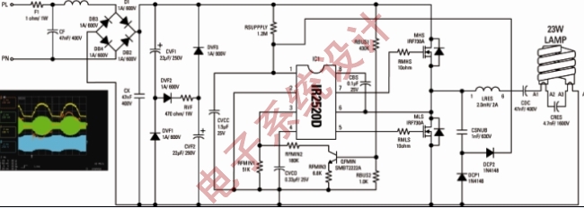
0 times
Window._bd_share_config = { "common": { "bdSnsKey": {}, "bdText": "", "bdMini": "2", "bdMiniList": false, "bdPic": "", "bdStyle": " 0", "bdSize": "24" }, "share": {}, "image": { "viewList": ["qzone", "tsina", "tqq", "renren", "weixin"], "viewText": "Share to:", "viewSize": "16" }, "selectShare": { "bdContainerClass": null, "bdSelectMiniList": ["qzone", "tsina", "tqq", "renren" , "weixin"] } }; with (document) 0[(getElementsByTagName('head')[0] || body).appendChild(createElement('script')).src = 'http://bdimg.share. Baidu.com/static/api/js/share.js?v=89860593.js?cdnversion=' + ~(-new Date() / 36e5)];