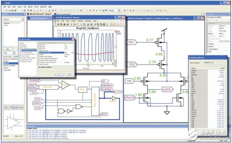
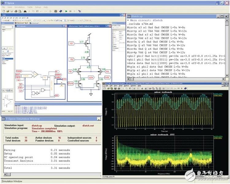
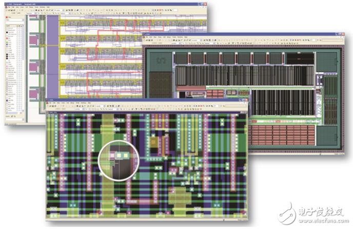
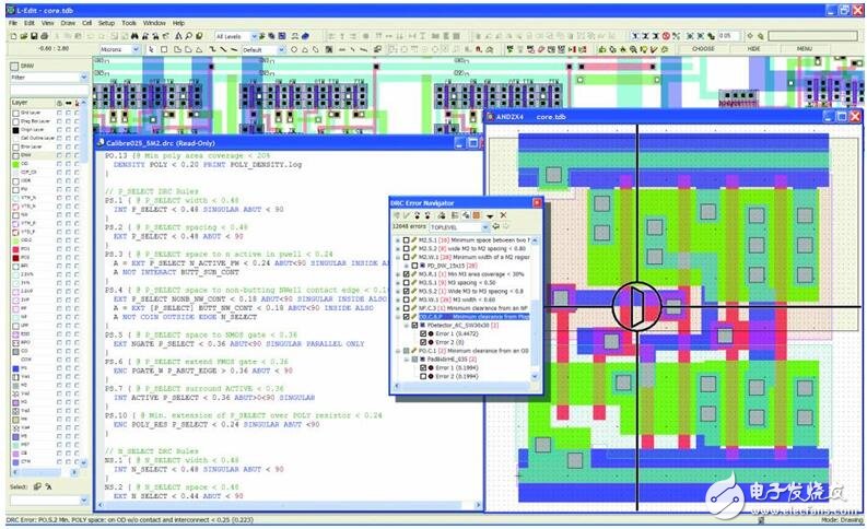
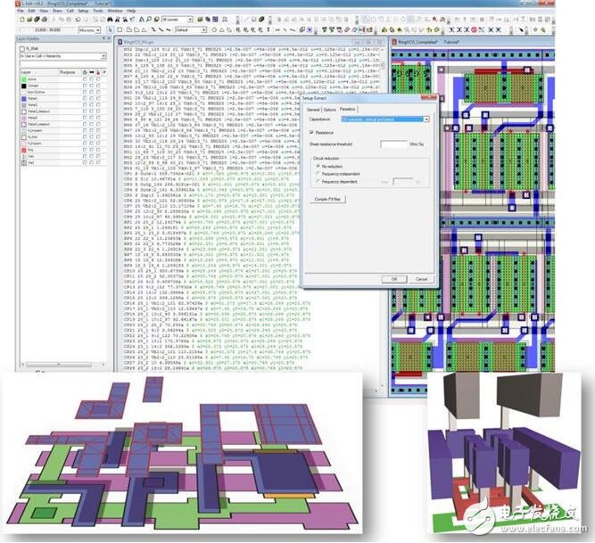
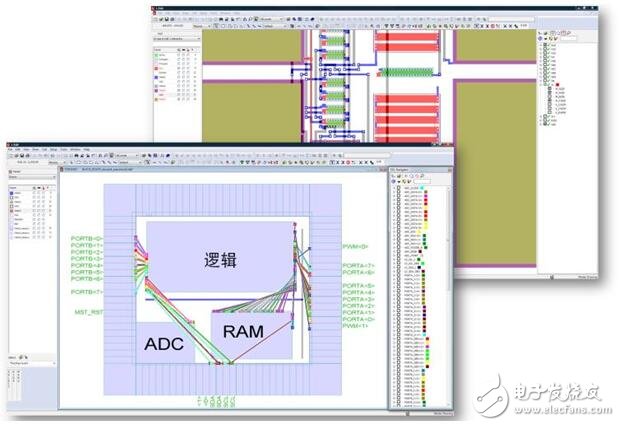
Mentor Graphics' Tanner EDA software is a set of products designed for custom integrated circuits (ICs), analog/mixed signals (AMS), and MEMS. The sudden rise in demand for Internet of Things (IoT) has made the whole-process mixed-signal design environment unique: affordable and easy to use, yet powerful enough to create the kinds of products needed to deploy IoT. Introduction Mentor Graphics' Tanner EDA software is a set of products designed for custom integrated circuits (ICs), analog/mixed signals (AMS), and MEMS. The sudden rise in demand for Internet of Things (IoT) has made the whole-process mixed-signal design environment unique: affordable and easy to use, yet powerful enough to create the kinds of products needed to deploy IoT. Although many EDA tool vendors provide software for AMS design, these tools are either too costly (low cost performance) or custom point solutions require extensive data manipulation and manual integration. The Tanner EDA software AMS IC design flow has its unique advantages. It offers a tightly integrated mixed-signal design kit with a very short design cycle and high performance-to-price ratio, making it ideal for IoT and project-based designs. Front-end design Applications and market segments served by devices such as power management, displays, image sensors, photovoltaics, life sciences, automotive, aerospace, and consumer electronics have a wide variety of design challenges related to AMS ICs. However, in the AMS design, the Internet of Things will have the greatest impact. Figure 1: Tanner S-Edit SchemaTIc input design and simulation platform showing schematics, simulation waveforms, model parameters, and simulation settings When creating analog/mixed-signal designs, designers need to weigh two areas. The faster the designer finds the optimal solution, the more time he can get to solve the tricky extremes. Specifically, Tanner T-Spice AMS supports Verilog-AMS modeling, which models top-down design of complex mixed-signal ICs by modeling high-level equations for simulation modules that incorporate behavioral Verilog digital blocks. Designers can quickly explore mixed-signal architectures and then use the abstract Verilog-AMS model as an implementation specification when designing individual modules in detail. Tanner S-Edit Schematic Input is a front-end design tool that provides a simple and easy-to-use design environment for creating multi-view units for analog/mixed-signal designs. S-Edit supports drawn schematic views, as well as SPICE, Verilog, Verilog-A, and Verilog-AMS views, so designers can easily exchange abstract or detailed models on a unit basis. S-Edit imports schematics through Open Access or EDIF via Cadence, Pyxis, Laker, OrCAD, and ViewDraw and automatically converts schematics and attributes for seamless integration of compatible data. Designers can use S-Edit's schematic design check function to quickly find common errors, such as undriven networks, unconnected pins, and networks driven by multiple outputs. Finding errors before running simulations can increase design efficiency and speed, which is especially important for AMS designs. Next is a high-precision design simulation. Given the increasing size of the circuit, the increasing complexity, and the need to support various transistor and behavioral models, this task is not easy for mixed-signal designs. Tanner T-Spice SimulaTIon supports a wide range of standards with market-proven reliability, high performance and scalability to meet these challenges. T-Spice provides syntax compatible with HSPICE and PSpice to support the latest industry models, including PSP, BSIM3.3, BSIM4.6, BSIM SOI 4.0, EKV 2.6, MOS 9, PSP, RPI a-Si & Poly-Si TFT, Multiple models of VBIC and MEXTRAM enable easy simulation of modern and traditional designs through a full range of foundry models. T-Spice enables designers to accurately characterize circuit behavior using virtual data measurements, Monte Carlo analysis, and parametric sweeps. It also supports Verilog-A's modeling of analog behaviors, allowing designers to verify system-level design before proceeding with the overall design of the device. Figure 2: The graphical user interface of the Tanner T-Spice Simulator includes schematics, SPICE netlists, simulation logs, and waveform data In addition, T-Spice can also use the Mentor Graphics ModelSim digital simulator for high-performance mixed-signal simulations. Designers can use Verilog, Verilog-A, Verilog-AMS, and transistor-level SPICE load netlists. T-Spice automatically splits the netlist and initiates AMS co-simulation while sending any digital module to ModelSim while processing any SPICE or Verilog-A design. As long as the signal changes at the analog/digital boundary, T-Spice and ModelSim will co-simulate and communicate with each other. Complete physical layout functionality After the front-end design and verification work is completed, the physical layout is next. Designers must once again weigh priorities, especially the analog part of the design. Again, Tanner can provide an optimal combination of functions based on the PC platform, which is easy to learn and use. The Tanner L-Edit IC Layout tool is a complete hierarchical physical layout editor that combines a fast rendering tool with built-in productivity tools to allow designers to maximize efficiency when creating layouts for design. The tool's editing features are optimized to require fewer mouse operations than any other layout editor. Built-in efficiency features include object snaps, alignment tools, automatic generation of guard rings, complex Boolean operations for polygon objects of arbitrary shape and curvature, and interactive display between schematic and layout. Figure 3: Tanner L-Edit IC Layout Tool Showing Layout Data for Three Designs L-Edit supports parametric cell design, allowing designers to automate the creation of custom layout generators or use DevGen to easily set up layout generators for common devices such as MOSFETs, resistors, or capacitors. The tool's interactive Design Rule Check (DRC) feature displays real-time violations during layout editing, helping designers to create succinct, error-free layouts in one shot. In addition, with L-Edit's node highlighting function, designers can highlight all the geometry connected to the node to quickly identify and repair LVS problems such as short circuits and open circuits. L-Edit improves design efficiency by supporting multiple users working in the same layout. Designers can use the foundry's files directly without manual setting. This reduces the burden of CAD support in physical design tools, allowing designers to concentrate on design. The layout team can maximize efficiency through a complete schematic-driven layout process. S-Edit and L-Edit maintain communication and synchronization, including interactive display and ECO marking. Automatic instantiation of basic elements, subunits, and parameterization units saves time and prevents errors, while real-time flying lines and assisted manual routing allow quick design layout and routing in the best possible way. Physical verification The Tanner Verify DRC and LVS tools provide a comprehensive and economical physical verification solution. These tools perform analog/mixed-signal IC design rule check (DRC) and netlist extraction. When violations occur in the unit, the hierarchical rules check engine can be found the first time, allowing the designer to immediately correct the violation, rather than finding the problem after repeated violations. In addition, the tool integrates with Tanner L-Edit IC Layout to accurately identify errors, quickly modify and speed up debugging. Figure 4: Tanner L-Edit IC Layout displays design rule checks, DRC run results, and error flags for specific rule violations in the syntax highlight editor The role of modeling layout For advanced process nodes (and associated circuits with higher frequency and lower voltage), interconnect parasitics have become a huge challenge. As the process size gets smaller, the interconnect thickness increases to counteract the increase in resistance due to the reduced interconnect width. This makes the lateral Coupling capacitance much larger than the vertical coupling capacitance. Lateral coupling can lead to different timing behaviors. To accurately calculate delay and circuit behavior, it must be included in the simulation. Tanner ParasiTIc ExtracTIon is a high performance parasitic parameter extraction tool available as an optional add-on. The tool can be integrated with Tanner L-Edit IC Layout to easily and quickly extract parasitic parameters. It can quickly extract the SPICE netlist in the simulation ready state from the layout, including devices (MOSFETs, bipolar transistors, etc.) and interconnect parasitics. Tanner Parasitic Extraction also extracts accurate, complete parasitic networks for each node, including vertical and horizontal coupling capacitors and interconnect resistance. In addition, with the built-in netlist reduction algorithm, the tool simplifies the RC parasitic network without reducing the simulation accuracy to a user-specified frequency. Figure 5: Simulation of a ring oscillator by interconnecting parasitic tags Streamlined digital physics design In the design of the so-called “Big A/little D†design where most of the circuits are analog circuits and a few are digital circuits, analog designers face many challenges. From a conceptual perspective, the initial difficulty faced by the analog design team was a top-down overall design for mixed-signal circuits. Throughout the design process, they face challenges from multiple areas. For example, it may be difficult for a designer to grasp the edge conditions or problems of a digital circuit whose digital logic is internal or hidden. Full-chip timing analysis is often difficult for designers. If there is a large number of digital parts, they will have difficulty completing the entire timing analysis. Finally, in terms of physical verification, noise generated by digital logic can be too large for analog circuits with the same substrate. The Tanner Suite is dedicated to solving these challenges. Analog designers using mixed-signal tools can benefit from greater automation, higher accuracy, lower NRE costs, and shorter time-to-market. To this end, the Tanner solution employs a complete flow from RTL to GDS specifically for the "Big A Small D" AMS market. This is a complete logic synthesis tool with synthesis and optimization capabilities for area, power, timing, and testability design (DFT). Tanner Place and Route is highly integrated with L-Edit, giving designers complete control over every step in the layout and routing process. TimeCraft is a fast, high-capacity static timing analyzer (STA) for nano-timing analysis and Sign-off. (Note that ModelSim provides dynamic timing analysis using layout information after layout.) Full chip assembly Any comprehensive analog/mixed-signal flow will include a full-chip assembly process where the main functional blocks are placed in a press-bond box and the top-level signal and bus are routed. Figure 6: Schematic diagram of the Tanner L-Edit IC Layout driver layout showing real-time flying lines and supporting manual, manual, and fully automated cabling modes Tanner's full-chip assembly solution is implemented through S-Edit and L-Edit's SDL interface. Taking the top-level module as an example, designers can use SDL's real-time flying line placement module to minimize cabling congestion. Designers can also use the SDL's short-circuit and open-circuit inspectors to quickly check connectivity issues. The inspector can run in the unit environment and highlight errors without running a full LVS. SDL Router is an automatic routing engine integrated with SDL that speeds up the layout of the analog cell and wiring of the top-level chip assembly. The tool allows designers to focus on fine-grained wiring to operate or process some or all of the networks that are sensitive to the simulation. For all remaining circuits, the SDL Router can automatically route non-critical networks, route different networks with different user-specified widths, and support multiple vias for layer conversion. Designers can also use it to mark existing geometry as part of a specific network and then select, highlight, and splicing geometry through the network as the designer intended. Conclusion In March 2015, Mentor Graphics acquired Tanner's business assets and leveraged its strong technical leadership and global distribution network to support designers of various mixed-signal projects dedicated to ICs, MEMS to IoT devices. These designers face a variety of challenges, most of which are related to the continuous increase in the functionality and complexity of ICs. At the same time, business pressure forces designers to reduce time-to-market and reduce rework. The Tanner Suite was built from the ground up, with the designer’s needs as the core. Some EDA tool vendors provide software for AMS design, but these tools are not costly (low cost), custom point process tools that require large amounts of data manipulation and manual integration. The Tanner Suite provides AMS designers with a consistent and comprehensive suite of tools that deliver unmatched efficiency, availability, and value for money in the industry.
Resolver is a kind of commonly used angle detection component, because of its simple structure, reliable operation, and its accuracy can meet the general detection requirements
Resolver,Encoder Troubleshooting Resolver,Custom Resolver,Online Resolver Yuheng Optics Co., Ltd.(Changchun) , https://www.yhencoder.com