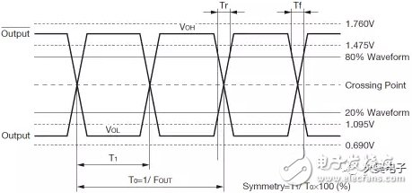
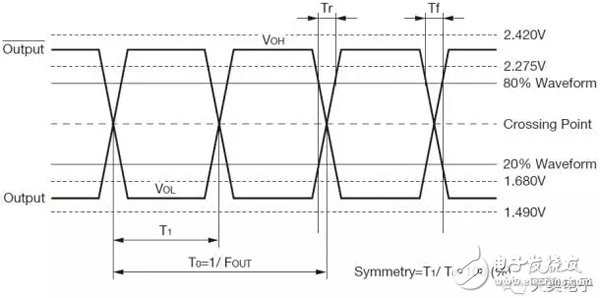
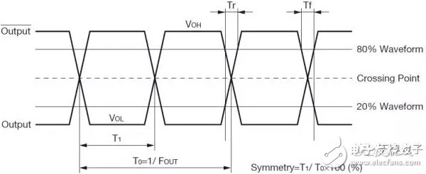
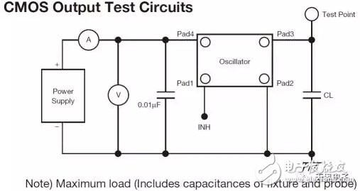
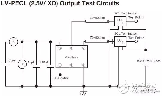
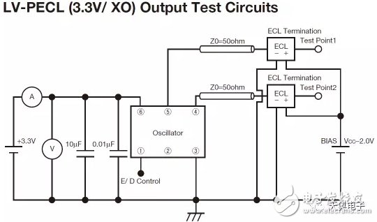
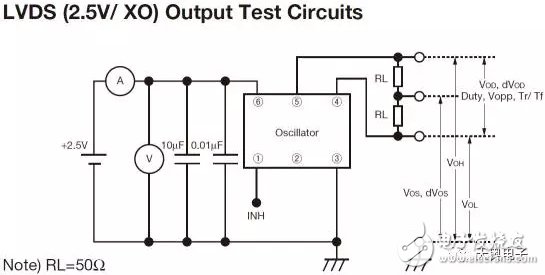
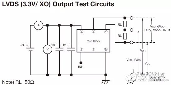
When we select and purchase a quartz crystal oscillator, or when we look at the crystal specifications provided by the manufacturer, there is an output type or output waveform. Frequently seen output modes are CMOS, TTL, Sine Wave, etc. What do these output modes mean? When we buy, how can we choose the right one? Let's take a look at the various output modes of the crystal oscillator below. Crystal oscillator commonly used output modes include: TTL, CMOS, ECL, PECL, LVDS, Sine Wave. These waveforms are commonly used waveforms in the industry. Among them TTL, CMOS, ECL, PECL, LVDS belong to square wave, Sine Wave belongs to sine wave. In general, the square wave output power is large, the driving ability is strong, but the harmonic wave component is abundant; The sine wave output power is not as good as the square wave, but its harmonic wave component is much smaller. Let us introduce the definition of these output modes one by one: (1) TTL: Transistor-Transistor Logic (Transistor-Transistor Logic) has a fast transmission delay time and high power consumption and is a current control device. (2) CMOS: Complementary Metal Oxide Semiconductor (Complementary Metal Oxide Semiconductor CMOS logic circuit), slow transmission delay, low power consumption, are voltage control devices. CMOS has greater noise tolerance relative to TTL and the input impedance is much larger than the TTL input impedance. Corresponding to 3.3V LVTTL, LVCMOS appears and can be directly driven with 3.3V LVTTL. HCMOS uses a fully static design, a high-speed complementary metal-oxide-semiconductor process, and CMOS uses a complementary metal-oxide semiconductor. CMOS will eventually be replaced by HCMOS. (3) ECL: Emitter-Couple Logic (Emitter-Couple Logic). This circuit is characterized in that the basic gate circuit operates in a non-saturated state. The ECL circuit has a rather high speed and the average delay time can reach several nanoseconds or even sub-nanoseconds. The logic swing of the ECL circuit is small (only about 0.8V, while the logic swing of the TTL is about 2.0V). When the circuit transitions from one state to another, the charge and discharge time for the parasitic capacitance will decrease. This is an important reason why the ECL circuit has a high switching speed. However, the logical swing of the ECL output is small, which is disadvantageous to the anti-jamming capability. In addition ECL circuit has a very high input impedance and low output impedance. (4) PECL: PosiTIve Emitter-Couple Logic (Positive Emitter-Couple Logic). The ECL circuit has a high speed, a strong driving ability, and a low noise, and it is easy to reach an application of several hundred MHz, but it consumes a large amount of power and requires a negative power supply. To simplify the power supply, the output modes of PECL (ECL structure, switching to positive voltage supply) and LVPECL appear. LVPECL is Low Voltage PosiTIve Emitter-Couple Logic. LVPECL is developed from ECL and PECL. The typical output of LVPECL is a pair of differential signals. Their emitters are grounded through an AC source. ECL, PECL, LVPECL should pay attention when using: Different levels can not be driven directly, the middle can use AC coupling, resistance network or special chip to convert. The above three are all emitter-to-output structures and must have a resistor to pull a DC bias voltage. (For example, if LVPECL is used for clocks, it will use 130 ohm pull-ups for DC match and 82 ohm pull-downs for dc match; 82 ohm pull-ups for AC match and 130 ohm pull-downs, but the DC level will be 1.95V after both operations. about.) (5) LVDS: Low-Voltage Differen TIal Signaling, which is a differential pair input and output. There is a constant current source of 3.5 to 4mA inside. It changes the direction and level on the differential line to indicate "1" and "0". ". It is converted to ±350mV differential level by an external 100Ω matching resistor (parallel connected on the differential line near the receiving end). LVDS use Note: can reach 600MHz or more, PCB requirements are higher, differential line requirements are strictly equal length, the difference is best not more than 10mil (0.25mm); 100 European resistor distance from the receiving end can not exceed 500mil, preferably controlled within 300mil. LVDS application mode can have three forms: 1 unidirectional point-to-point and bidirectional point-to-point, two-way half-duplex communication can be achieved through a pair of twisted pair; 2 multi-branch form, that is, a driver to connect multiple receivers (when the same This application can be used when the data is to be transmitted to multiple loads.) 3 Multi-point architecture, where the multi-drop bus supports multiple drivers, or BLVDS drivers, which can provide bi-directional half-duplex communication but are At a time, only one driver can work. Therefore, the priority of sending and the arbitration protocol of the bus need to use different software protocols and hardware solutions according to different application occasions. (6) Clipped Sine Wave: Clipped Sine Wave. Compared with the square wave, the harmonic components are much less, but the driving ability is weak. When the load is 10K//10PF, Vp-p is 0.8Vmin. The output waveforms for the surface mount crystal oscillator are usually SMD 7050, SMD5032, and SMD3225. (7) Sin Wave: Generally, the load impedance of the crystal sine wave output is 50 ohms. The harmonic components of the waveform are small, and the general harmonic suppression is better than -30 dBc. Sine wave output crystals are commonly used in RF signal processing, frequency sources and other applications. After understanding these definitions, according to the actual use situation, TTL is generally not used due to high power consumption. We do not analyze TTL any more here. Below, we take a look at the actual test results of the output waveform to see the difference between several square wave output waveforms: (1) CMOS: (2) LVPECL (@2.5V): (3): (4) LVDS: Through the output of the waveforms of the above output modes, we can also see the difference between them. Here we tell about the test circuit of each circuit: (1) CMOS output test circuit: (2) LVPECL output (@2.5V) test circuit: (3) LVPECL output @ 3.3V test circuit: (4) LVDS output (@2.5V) test circuit: (5) LVDS output (@3.3V) test circuit: Through the above analysis, I believe we have a certain understanding of the differences between the output modes. Furniture Zinc Alloy Die Casting Furniture Zinc Alloy Die Casting,Die Aluminium Zinc Casting,Black E Cigarette Charger Casting,Power Tool Aluminum Housing Dongguan Metalwork Technology Co., LTD. , https://www.dgdiecastpro.com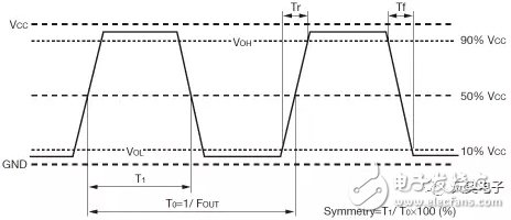
Summary