Various PCB tests are an inspection method to discover problems in time, and it is also a necessary means to prevent more defective products and reduce losses. General test list Operation process and operation requirements: 1. Browning peel strength test: 1.1 Test purpose: to determine the peel strength of browning 1.2 Equipment supplies: 1OZ copper foil, substrate, tensile tester, blade 1.3 Test method: 1.3.1 Take a substrate with an appropriate area and etch away the copper foil on both sides. 1.3.2 Take a piece of 1OZ copper foil of the same size and fix it on the substrate. 1.3.3 Operate the above samples according to the browning→pressing process. When the PP is pressed and laminated, the browned surface of the copper foil is in contact with the PP. 1.3.4 Cut out suitable samples after pressing, and cut the copper foil on the board surface with a blade into two parallel lines, about 10cm in length and ≧3.8mm in width. 1.3.5 Test the peel strength of the copper foil according to the operating specifications of the tensile tester. 1.4 Calculation: 1.5 Sampling method and frequency: take the test board 1PCS/line/week 2. Slice test: 2.1 Test purpose: to press the thickness of a dielectric layer; Drill a hole to test the roughness of the hole wall; Plating a precise control of copper plating thickness; Anti-welding-thickness of green oil; 2.2 Equipment supplies: sandpaper, grinder, metallographic microscope, polishing liquid, micro-etching liquid 2.3 Test method: 2.3 Test method: 2.3.1 Select the sample and punch out the slices at the appropriate position with a punch. 2.3.2 Fix the slice vertically in the model. 2.3.3 Mix the resin and hardener in proportion and pour it into the model to make it harden naturally. 2.3.4 Use sandpaper to coarsely grind from small mesh to large mesh and finely grind to a position close to the center of the hole 2.3.5 Polish with polishing liquid. 2.3.6 Micro-etched copper surface. 2.3.7 Observe and record with a metallurgical microscope. 2.4 Sampling method and frequency: Electroplating-first piece, 1PNL/per cylinder/per shift, independent piece 2PNL/per batch, 9 points for hole copper measurement, 9 points for C\S surface when measuring surface copper. Drilling-the first piece, (1PNL/axis/4 machines/shift, take the bottom plate of the drilling plate) to cut the position of the edge of the plate, and read the maximum hole wall roughness value. Pressing-the first piece, (1PNL for each material number and when the thickness of the test plate is unqualified), take any position on the edge of the pressing plate. (Note: The thickness of the laminated dielectric layer is allowed to be less than or equal to 1mil than the required value.) Anti-welding-the first piece, (1PNL/4 hours) take an independent circuit. 3. Soldering tin/resistance test for repairing wire: 3.1 Test Purpose: To predict the quality of the product patch line after soldering and the resistance value of the patch line. 3.2 Instrument supplies: oven, tin furnace, stopwatch, flux, metallographic microscope, ohmmeter, repair knife. 3.3 Test method: 3.3.1 Select the sample and put it in the oven to bake at 150°C for 1 hour. During the operation, wear roving gloves and use a long handle to pick and place the sample. 3.3.2 Take out the sample and let it cool to room temperature. 3.3.3 Apply the flux evenly and drip it upright for 5-10 seconds to allow the excess flux to drip back. 3.3.4 Completely immerse the tin liquid in the tin furnace at 288℃±5℃ for 10±1 seconds/time, 3 times (the patch wire must be completely immersed). After each tin immersion, cool down and then re-immerse. 3.3.5 After the test, clean the sample to check whether the patch cord is off. 3.3.6 If the section at the patch line cannot be judged, use a metallurgical microscope to check whether there is any abnormality at the patch line. 3.4 Resistance value test method: 3.4.1 After patching the wire, use a repair knife to scrape off the coverings (solder resist, copper oxide layer) at both ends of the patching wire, and do not damage the copper surface. 3.4.2 Use an ohmmeter to measure the resistance value at both ends of the compensation line. 3.4.3 Sampling method and frequency: Take 1PCS each of the finished and semi-finished boards/week/each line operator 4. Green oil dissolution test: 4.1 Test purpose: to test whether the solder resist on the surface of the sample has been hardened and is sufficient to cope with the heat generated during welding. 4.2 Equipment supplies: chloroform, stopwatch, rags 4.3 Test method: 4.3.1 Put a few drops of chloroform on the surface of the solder mask of the sample and wait for about one minute. 4.3.2 Use a rag to wipe off the place where the chloroform has been dripped. The cloth surface should not have the color of solder resist. 4.3.3 Use your fingernail to scrape it off at the same position. If the solder resist is not scraped, it means the test is qualified. 4.4 Sampling method and frequency: 3pcs/each batch before shipment 5. Acid and alkali resistance test: 5.1 Test purpose: to evaluate the acid and alkali resistance of green oil. 5.2 Equipment: H2SO4 10% NaOH 10% 600#3M tape 5.3 Test method: 5.3.1 Prepare an appropriate amount of H2SO4 with a concentration of 10%. 5.3.2 Prepare an appropriate amount of NaOH with a concentration of 10%. 5.3.3 Put the sample in an oven and heat it to about 120±5°C for 1 hour. 5.3.4 Soak the two groups of samples in each of the above solutions for 30 minutes. 5.3.5 Take out the sample and wipe it dry. Use 600#3M tape to stick to the paint surface with a length of about 2 inches. Wipe the surface with hands 3 times to ensure that the tape can only be used once at a time. 5.4 Sampling method and frequency: 3pcs/each batch before shipment Six, green oil hardness test: 6.1 Test purpose: to test the hardness of green oil. 6.2 Equipment: Standard hardness pencil: 6H pencil 6.3 Test method: 6.3.1 Sharpen the pencil with a sharpener and sharpen the tip with fine sandpaper. 6.3.2 Place the sample horizontally on the work surface, first use a 6H pencil on the surface of the sample with normal strength, tilt 45 degrees, and then push the pencil to the direction of the sample, so that the nib is drawn on the surface of the solder mask about 1/4" long . 6.3.3 If the solder mask is not scratched or damaged, it means that the hardness of the sample is >6H. 6.3.4 If the solder resist has scratch marks, the hardness 6.4 Sampling method and frequency: 3pcs/each batch before shipment Seven, green oil adhesion test: 7.1 Test purpose: to test the adhesion of the solder resist to the sheet or circuit surface. 7.2 Equipment supplies: 600#3M tape 7.3 Test method: 7.3.1 Before testing, check that the surface of the sample must be clean and free of dust or oil. 7.3.2 Use 600#3M tape to stick to the paint surface with a length of about 2 inches. Wipe the surface with hands 3 times to ensure that it is flat. The tape can only be used once at a time. 7.3.3 Pull up the vertical surface of the tape quickly by hand. 7.3.4 Check whether the adhesive tape is attached with solder resist and whether the solder resist on the board surface is loose or separated. 7.4 Sampling method and frequency: 3pcs/each batch before shipment 8. Thermal stress test: 8.1 Test purpose: to predict the thermal stress tolerance of the product at the customer 8.2 Equipment supplies: oven, tin furnace, stopwatch, flux, metallographic microscope. 8.3 Test method: 8.3.1 After selecting an appropriate sample on the surface to check that there is no delamination, blistering, or texture revealing, and the BGA and CPU have not been drawn with a whiteboard pen, put it in the oven and bake at 150°C for 4 hours. 8.3.2 Take out the sample and let it cool to room temperature. 8.3.3 Adjust the temperature of the tin furnace to 288℃, and insert the thermometer into the tin furnace to confirm the temperature of the tin furnace. If it does not meet the requirements, perform compensation until it meets the requirements. Then perform compensation until it meets the requirements. 8.3.4 Clamp the test board with a clamp, and apply the flux evenly on the board surface and drip it upright for 5-10 seconds to allow the excess flux to drip back. Take the drop back. 8.3.5 Completely immerse the tin liquid in the tin furnace at 288℃±5℃ for 10±1 seconds/time, take it out and cool it for the second time, total 3 times. 8.3.6 After taking out the sample, let it cool down, and clean the sample. 8.3.7 Make hole slices (make slice analysis according to the minimum diameter and PTH hole). 8.3.8 Use a metallurgical microscope to observe the section of the hole. 8.4 Precautions: Wear high-temperature gloves, sleeves and protective masks during operation, and use long-handled grippers to pick and place samples and test. 8.5 Sampling method and frequency: 3pcs/each batch before shipment Nine, lead solder test: 9.1 Test purpose: In order to predict the soldering condition of the product at the customer, use the Solder pot to simulate the soldering condition of the customer. 9.2 Equipment supplies: oven, lead tin stove, stopwatch, lead flux, 10X magnifying glass 9.3 Test method: 9.3.1 Select the appropriate sample. The BGA and CPU have not been drawn with whiteboard markers. After confirming that the surface of the sample is clean, put it in the oven and bake at 120℃*1 hour. 9.3.2 After taking out the sample, let it cool down to room temperature. 9.3.3 Completely remove the scum on the surface of the molten tin in the tin furnace and the coked flux residue. 9.3.4 Completely coat the sample with flux. The sample must be dripped upright for 5-10 seconds to allow the excess flux to drip back. 9.3.5 Place the sample carefully on the surface of the tin bath at a temperature of 245°C for a floating time of 3 to 5 seconds. 9.4 Precautions: Wear high temperature gloves, sleeves and protective masks during operation, and use long handles to pick and place samples and test. 9.5 Sampling method and frequency: 3pcs/each batch before shipment. 10. Lead-free solder property test: 10.1 Test purpose: In order to predict the soldering condition of the product at the customer, use the Solder pot to simulate the soldering condition of the customer. 10.2 Equipment supplies: oven, lead-free tin furnace, stopwatch, lead-free flux, 10X magnifying glass 10.3 Test method: 10.3.1 Select the appropriate sample, the BGA and CPU have not been drawn with whiteboard markers, and after confirming that the sample surface is clean, put it in the oven and bake at 120℃*1 hour. 10.3.2 After taking out the sample, let it cool down to room temperature. 10.3.3 Completely remove the scum and coked flux residue on the tin melting surface in the tin furnace. 10.3.4 Completely coat the sample with flux. The sample must be kept upright and drip for 5-10 seconds to allow the excess flux to drip back. 10.3.5 Place the sample carefully on the surface of the tin bath at a temperature of 260°C for a floating time of 3 to 5 seconds. 10.4 Matters needing attention: Wear high temperature gloves, sleeves and protective masks during operation, and use long handles to pick and place samples and test. 10.5 Sampling method and frequency: 3pcs/each batch before shipment. 11. Ion pollution degree test: 11.1 Test purpose: test the ion pollution degree of PCB after tin spraying, browning and molding. 11.2 Equipment supplies: ion pollution machine, isopropanol concentration 75±3% 11.3 Test method: Test according to the operating specifications of the ion pollution machine. 11.4 Matters needing attention: gloves must be worn during operation, and the board surface must not be polluted. 11.5 Sampling method and frequency: times/shift Take browning board 1 time/shift Take molding board 1 time/shift 12. Impedance test: 12.1 Test purpose: to measure whether the impedance value meets the requirements 12.2 Instruments and Supplies: Impedance Tester 12.3 Test method: Test according to the operating specifications of the impedance tester 12.4 Sampling method and frequency: Impedance requirements: dry film etching 1PNL per shift per part number per line first board, independent 2 PNL/batch, solder mask 3PNL per part number per shift (Note: The standard value of impedance after solder mask is the same as the standard value of finished product) 13. Tg test: 13.1 Test purpose: To test whether the Tg of the laminate meets the requirements. 13.2 Instruments and supplies: Tg tester. 13.3 Test method: Test in accordance with the operating specifications of the Tg tester. 13.4 Sampling method and frequency: take the finished board 1PCS/week. 14. Tin-lead composition test: 14.1 Test purpose: To check whether the tin-lead composition is within the acceptable range through testing. 14.2 Instruments and Supplies: Spectrovac 2000OR emission direct reading spectrum. 14.3 Test method: Outgoing test. 14.4 Sampling method and frequency: take tin samples for each line of spray tin/week. 15. Etching factor test: 15.1 Test purpose: to check the undercut condition of the etching line through the test. 15.2 Equipment supplies: sandpaper, grinding machine, metallographic microscope, polishing liquid, micro-etching liquid 15.3 Test method: etch according to normal parameters, then slice and analyze the etching factor calculation formula: EF=2T/(ba) 15.4 Sampling method and frequency: take the normal mass production board of the outer etching line, 1PCS/each line/month. 16. Chemical gold and text adhesion test: 16.1 Test purpose: to check the adhesion of the gold after the gold is melted through the test. 16.2 Instruments: 3M#600 tape 16.3 Test method: 16.3.1 Put the test board on the table 16.3.2 Use 600#3M tape to stick to the paint surface with a length of about 2 inches. Wipe the surface with hands 3 times to ensure that it is flat. The tape can only be used once at a time. 16.3.3 Use your hands to quickly pull up the vertical surface of the tape. 16.3.4 Observe whether there is gold/text paint on the tape, and whether the gold/text paint on the board surface is loose or separated. 16.3.5 Sampling method and frequency: 3pcs/each batch before shipment 17. Hole tension test: 17.1 Test purpose: to test the tensile strength of copper plated holes 17.2 Equipment supplies: electric soldering iron, tensile tester, copper wire 17.3 Test method: 17.3.1 Insert the copper wire directly into the hole and solder it with an electric soldering iron; 17.3.2 The tested hole must be intact on the PAD surface, and cut off the excess circuit on the PAD side; 17.3.3 Clamp the end of the copper wire with a tensile machine, and press the tensile machine up until the copper wire is broken or the hole is pulled out, and the reading C (Kg) is counted; 17.3.4 Use a vernier caliper to measure the inner diameter C2 (mm) of the hole and the outer diameter C1 (mm) of the hole ring. 17.3.5 Calculate the hole tensile strength: ib/in2 F = 4C/ (C12-C22)*1420 F: Tensile strength C1: Annular outer diameter (mm) C2: Annular inner diameter (mm) 17.3.6 Sampling method and frequency: take 1PCS/week of the outer etching board 18. Wire tension test: 18.1 Test purpose: To test the adhesion of the coating to PP. 18.2 Equipment supplies: tensile testing machine, blade, vernier caliper. 18.3 Test method: 18.3.1 Use a vernier caliper to measure the line width (mm). 18.3.2 Pick up the wire end with a blade and peel off about 2cm, and clamp the raised wire end with the chuck of a tensile tester. 18.3.3 Peel the line by ascending, (drawing rod speed: 50MM/MIN), gauge the reading of pulling force (Kg). 18.3.4 Line tension calculation: Tensile force (kg) Unit: ib/in Line width (mm) Unit: ib/in 18.4 Sampling method and frequency: Take 1PCS/week of the outer etching board. 19. High voltage insulation test: 19.1 Test purpose: test the insulation performance of circuit board materials 19.2 Equipment supplies: high voltage insulation tester, oven 19.2 Equipment supplies: high voltage insulation tester, oven 19.3 Test method: 19.3.1 Bake the board at a temperature of 50-60℃/3 hours, and cool to room temperature. Select the pair of wires that are closest to each other and are not connected to each other on the sample. 19.3.2 Test according to the operating specifications of the high-voltage insulation tester, the test requirements are: a) Line spacing b) Line spacing ≧3mil, required voltage 500V, current 0.5A. c) The voltage and current can be set according to customer requirements. d) Or use 1000V for double-sided boards and 500V for multi-layer boards. 19.3.3 Keep the power on for 30+3/-0 seconds. If there is a breakdown during this period, it means that the sample is unqualified. 19.3.4 Before the test, the test table must be cleaned, and there must be no metal objects, so as not to affect the test results or electric shock. 19.4 Matters needing attention: wear high pressure gloves during operation 19.5 Sampling method and frequency: 1PCS/cycle of the finished board Twenty, spray tin (gold, gold, silver) thickness test: 20.1 Test purpose: to check whether the thickness of sprayed tin (metallurgical gold, silver) is within the acceptable range. 20.2 Instruments and Supplies: X-Ray Tester 20.3 Test method: Test according to the X-Ray tester operating specifications. 20.4 Sampling method and frequency: first piece, 1pcs/each batch 21. Abnormal management and troubleshooting: 1. If the reliability test of the finished product finds that 1pcs is unqualified, it should be reported to the quality assurance supervisor immediately, and the board with the same material number and the same period should be re-doed the same reliability test (amount above 10pcs), such as 1pcs board in the second test Repeat the same reliability test (amount 10pcs or more) for the board that fails the test. For example, in the second test, 1pcs board fails the test and discuss the follow-up rework and reinspection countermeasures. 2. If there is a failure to test 1pcs in the manufacturing process, it is necessary to immediately report to the quality assurance supervisor and the responsible unit supervisor, and take the same material number and the same cycle board to retry the test (the quantity is more than 5pcs), and there is 1pcs board test in the second test The unqualified CAR shall be issued to the responsible unit, and after the improvement, the results will be confirmed by sampling. Twenty-two, welding quality inspection: 1. Check directly visually, and then check with a magnifying glass of 1.5-10 times. 2. Adhesion (tape test): According to the provisions of TM2.4.28.1 in IPC-TM-650, use 3M tape to test the peel strength of the coating film. 3. Hardness test: According to IPC-SM-840C 3.5.1/TM 2.4.27.2 standard for hardness test, use a piece of post-baked board, use a pencil hardness meter (JIS standard) to form an angle of 45℃ with a force of about one newton. Draw a line about one inch long on the surface, wipe off the toner with a rubber, and check for scratches on the board, as long as the scratches do not reveal copper. 4. Acid and alkali resistance test: According to IPC-SM-840C 3.6.1.1 standard, take 2 pieces of each 6PNL silver test plate and immerse each of them in 10% HCl, 10% H2SO4, 10% NaOH solution for 30 minutes; take another 6PNL OSP test plate each After immersing 2 pieces in 10% HCl, 10% H2SO4, 10% NaOH for 60 minutes, observe whether there is blistering, peeling, discoloration, etc. on the surface, and then use 3M tape for peeling test 5. Solvent resistance: According to IPC-SM-840C 3.6.1.1 standard, clean the surface of the coating film, observe whether there is blistering, peeling, discoloration, etc. on the surface, and then use 3M tape for peeling test 6. High temperature resistance: 1) Weldability: When welding according to IPC-SM-840C3.7 and J-STD-003, check whether there is any adverse effect on the weldability of the solder joint. 2) Solder resistance: According to IPC-SM-840C3.7.2, according to the specified conditions (J-STD-004: M flux, J-STD-006: Sn60 or Sn63 type solder), check for solder paste adhesion after soldering于coating. 3) Solder heat resistance: After soldering, observe the appearance of the coating film to check for blistering; after applying the tape pull test, check for peeling and other defects 4) Spray tin resistance: After spraying soldering flux before spraying tin, check whether the coating film has blistering, peeling, etc., and then apply the tape pull test to observe the appearance of the coating film. 5) Bleaching tin test: temperature: 260℃, time 10S, test three times; 288℃, time 10S, test three times. Afterwards, check whether the coating film has blistering or peeling. 7. Check the plug hole effect: take the board and cut the BGA bit to make several slices to check the plug hole effect. 8. Detect the ink thickness on the circuit: take the silver and OSP board into slices, and measure the ink thickness at different positions on the circuit. 9. Undercut side erosion situation: Take the test board to make several slices, and measure whether the depth of the undercut is within the specified range of 1.2mil. 10. Thermal shock resistance: According to IPC-SM-840C 3.9.3/TM2.6.7.1 H grade -65~125°C, 100 cycles, check the coating film for blistering, cracking, peeling, etc. 11. Chemical resistant silver, OSP, and gold plating/chemical gold performance: Take a few test plates after different surface treatments of chemical silver and OSP wires in a factory, and observe whether there are any bad conditions such as blistering, peeling, arching or discoloration. (Test conditions-gold plating (electrolysis): 42°C, 1.0A/dm², 5 minutes; gold (no electrolysis): 90°C, 5 minutes.)
UCOAX specializes in custom drawing, flattening, stranding and insulating, cutting and stripping of fine wire and cable .0009" (AWG #48) and larger.
UL iQ for appliance wiring materials
Single-Conductor, Themoplastic Insulation
1007 1015 1061 1185 1126 1227 1330 etc.
Multiple-Conductor, Thermoset Insulation
2464 2468 2725 2835 2990 20276 20379 21100 21118
Single-Conductor, Thermoset Insulation
3173 3265 3266 3271 3272 3302 3346 3347 3363 3383 3385 3386 3619
For more details, please feel free to contact us, thank you.
Ul Wiring Material,Ul Wiring Material Components,Electrical Wire Materials,Wiring Material UCOAX , https://www.ucoax.com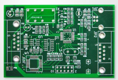
Serial number content General control standards 1 Browning peel strength test Peel strength ≧3ib/in 2 Slice test 1. According to customer requirements; 2. According to the production flow sheet requirements 3 Copper plating thickness 1. According to customer requirements; 2. According to the production flow sheet requirements 4 Repair wire solder, the resistance change rate does not fall off or separate, Resistance change rate≦20% 5 Green oil dissolution test The white cloth does not stick to the color of the solder mask, and the solder mask is not scratched 6 Green oil acid and alkali resistance test Text, green oil without peeling or delamination (excluding UV text) 7 Green oil hardness test Hardness>6H pencil 8 Green oil adhesion test No shedding and separation 9 Thermal stress test (immersion tin) No bursts and holes 10 (Lead-free) solderability test More than 95% of the tin is well dipped, the others can only show pinholes and tin shrinkage 11 (With lead) solderability test More than 95% of the tin is well dipped, the others can only show pinholes and tin shrinkage 12 Ion contamination test ≦4.5μg.Nacl/sq.in (browning board), ≦3.0μg.Nacl/sq.in (molding, spray tin) finished products are shipped according to customer requirements 13 Impedance test 1. According to customer requirements; 2. According to production process sheet requirements 14 Tg test Tg≧130℃,△Tg≦3℃ 15 Tin lead composition test According to customer requirements 16 Etching factor test ≧2.0 17 Chemical gold/text adhesion Test without falling and separation 18 Hole tension test ≧2000ib/in2 19 Wire tension test ≧7ib/in 20 High voltage insulation test No breakdown twenty one Spray tin (gold, gold, silver) thickness test According to customer requirements