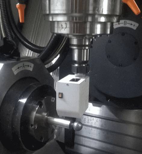
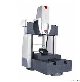
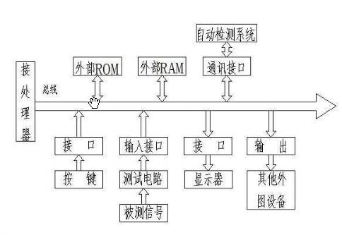
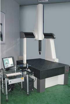
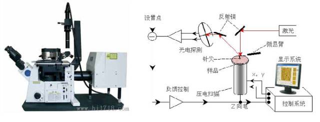
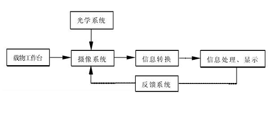
Today, with the rapid development of science and technology, modern precision measurement technology plays an important role in the development of a country. Without advanced measurement techniques and measurement methods, it is difficult to design and manufacture products with excellent comprehensive performance and single-phase performance, let alone develop modern high-tech cutting-edge technologies. Therefore, all industrialized countries in the world attach great importance to and develop modern precision. Measurement technology. Precision coordinate measurement Precision measurement technology Modern precision measurement technology is a comprehensive interdisciplinary subject integrating optics, electronics, sensors, imaging, manufacturing and computer technology. It covers a wide range of subject areas and its development requires the support of many related disciplines. In modern industrial manufacturing technology and scientific research, measuring instruments have a development trend of precision, integration and intelligence. The Coordinate Measuring Machine (CMM) is a typical representative of the above-mentioned development trend. It can measure high-accuracy of almost all dimensions, shapes and mutual positions of all three-dimensional complex parts in production. The development of high-speed coordinate measuring machines is a requirement of modern industrial production. At the same time, as a key development goal of the next century, countries have carried out extensive application research in the field of micro/nano measurement technology. Coordinate measuring machine The coordinate measuring machine is widely used as a geometric digital measuring device in the field of mechanical manufacturing. 1. Error self-compensation technology The CNC small coordinate measuring machine developed by Carl Zeiss of Germany adopts the thermal insensitive ceramic technology, so that the measurement accuracy of the coordinate measuring machine is not affected by the temperature change in the range of 17.8-25.6 °C. The domestically developed CNC measuring machine software system PMIS includes a number of system error compensation, system parameter identification and optimization techniques. CNC small coordinate measuring machine 2, rich software technology The coordinate measuring machine software STRATA-UX developed by CarlZeiss can directly transfer the measurement data from the CMM to the statistical software equipped with it, analyze and manage the inspection data given by the measurement system in real time, and evaluate it according to the requirements. According to this database, various statistical reports can be automatically generated, including X-BAR&R and X_BAR&S charts, frequency histograms, running charts, target charts, and so on. The US company's Cameleon measurement system is equipped with support software that provides more than 50 measurement modules including gears, plates, cams and camshafts. Japan's Mistutor has developed a graphical display and mapping program to assist the operator in comparing actual values ​​with required measurements, with multiple output methods. STRATA-UX system processing diagram 3. Non-contact measurement A non-contact laser optical probe based on the principle of triangulation is applied to the CMM instead of the contact probe. The surface roughness information can be accurately obtained by scanning the probe, and the three-dimensional measurement of the surface contour and the identification of the mold characteristic line are performed. This method overcomes the limitations of contact measurement. The laser dual triangulation method is applied to a wide range of measurements, and the contour of a complex surface is measured with an accuracy of more than 1 μm. The IMP type coordinate measuring machine produced by British IMS company can be equipped with contact or non-contact probes provided by other manufacturers. IMP type coordinate measuring machine Micro/nano precision measurement technology Science and technology are developing in a small field, from millimeters and micrometers to nanoscales, ie micro/nano technologies. Nano-scale processing technology can be divided into two aspects: processing accuracy and processing scale. Machining accuracy has evolved from the highest precision micron scale at the beginning of this century to the existing nanometer order of magnitude. The precision of the ultra-precision diffraction grating processed by the diamond lathe has reached 1 nm, and it has been possible to make wires, columns and grooves of 10 nm or less. The development of micro/nano technology is inseparable from micron and nanometer measurement technology and equipment. Geometrical and surface topography measurement techniques with micron and submicron measurement accuracy are relatively mature, such as the HP5528 dual-frequency laser interferometry system (accuracy 10 nm), optical stylus profile scanning system with 1 nm accuracy. Because scanning tunneling microscopy, scanning probe microscopy, and atomic force microscopy are used to directly observe the realization of atomic-scale structures, processing at the atomic level, assembly, and reshaping has become a cutting-edge technology in recent years. 1, scanning probe microscope In 1981, the successful scanning tunneling microscope developed by IBM in the United States brought people to the microscopic world. It has a very high spatial resolution and is widely used in research fields such as surface science, materials science and life sciences, and promotes the generation and development of nanotechnology to a certain extent. At the same time, based on the similar principles and structures of STM, a series of scanning probe microscopes (SPM) have been developed that utilize different interactions between probes and samples to detect the properties exhibited by the surface or interface at the nanoscale. Various information about surface structure and properties that cannot be obtained through STM has become a powerful tool for human understanding of the microcosm. Below are several representative scanning probe microscopes. (1) Atomic Force Microscopy (AFM) In order to compensate for the defect that STM is limited to observing the surface structure of conductors and semiconductors, Binning et al. invented AFM. AFM uses micro-probes to drive high-sensitivity microcantilever to move up and down with surface undulations when the sample surface is scratched. Or the tunnel current detects the displacement of the microcantilever, and the repulsive force between the probe tip atom and the surface atom is detected, thereby obtaining surface topography information. For applications, STM is primarily used in natural science research, and a significant number of AFMs have been used in industrial technology. In 1988, the Institute of Chemistry of the Chinese Academy of Sciences successfully developed the first AFM with atomic resolution in China. A micro-fiber-conducting laser interference 3D measurement system is installed, and self-calibration and absolute measurement of the atomic force microscope can quantify the current nanometer measurement technology. Using the working principle similar to AFM, the effect of the measured surface characteristics on the forced vibration force sensitive component is detected. The electrostatic force, magnetic force, van der Waals force and the like existing on the surface of the sample can be detected in the range of the distance between the probe and the surface of 10 to 100 nm. Force, the development of magnetic force microscope, electrostatic force microscope, friction microscope, etc., collectively referred to as scanning force microscope. Atomic force microscope and working principle (2) Photon scanning tunneling microscope (PSTM) The principle and working mode of PSTM is similar to that of STM. The latter uses electron tunneling. The former uses photon tunneling to detect the instantaneous fading field excited by total internal reflection near the surface of the sample. Its intensity is a function of the distance from the interface. Obtain surface structure information. Photon scanning tunneling microscope (3) Other microscopes For example, scanning tunneling potential (STP) can be used to detect nanoscale potential changes; scanning ion conductivity microscopy (SICM) is suitable for biological and electrophysiological studies; scanning thermal microscopy has obtained the surface structure of red blood cells; ballistic electron emission microscopy (BEEM) is the only advanced analytical instrument capable of non-destructive testing of surface and interface structures at the nanoscale. It has also been successfully developed in China. Scanning tunnel potentiometer 2. Scanning X-ray interference technology for nanometer measurement SPM-based observation techniques can only give nano-scale resolution, but can not give accurate nano-size of surface structure, because there is no simple nanometer precision (0.10 ~ 0.01nm) size measurement. Standard means. The interplanar spacing of silicon (220) crystals measured by NIST and German PTB was 192015.560±0.012fm and 192015.902±0.019fm, respectively. The Japanese NRLM tested the stability of the 220 crystal pitch at a constant temperature and found that its 18-day variation did not exceed 0.1 fm. The experiment fully demonstrates that the interplanar spacing of single crystal silicon has good stability. Scanning X-ray interferometry is a new technology in micro/nano measurement. It uses the interplanar spacing of single crystal silicon as the basic unit of measurement for sub-nanometer accuracy, plus the X-ray wavelength is smaller than the wavelength of visible light. On the order of magnitude, it is possible to achieve a resolution of 0.01 nm. Compared with other methods, the method has low environmental requirements, good measurement stability and simple structure, and is a convenient nanometer measurement technology with great potential. Since DG Chetwynd applied it to micro-displacement measurement in 1983, English, Japanese, and Italian have applied it to the correction of nano-scale displacement sensors. In May 1997, the State Key Laboratory of Testing Technology and Instruments of Tsinghua University used X-ray interference devices developed by itself to observe X-ray interference fringes for the first time in China. Soft X-ray microscopy, scanning photoacoustic microscopy, etc. are used to detect micro-defects of microstructure surface topography and internal structure. Michelson-type beat interferometer for ultra-fine machining surface contour measurement, such as polished surface, lapping surface, measuring surface contour height variation of up to 0.5nm, lateral (X, Y-direction) measurement accuracy of 0.3 ~1.0μm. The Wollaston-type differential dual-frequency laser interferometer has a resolution of up to 0.1 nm in the measurement of microscopic surface topography. Michelson-type beat interferometer 3. Optical interference microscope measurement technology Optical interference microscopy measurement technology, including heterodyne interferometry, ultra-short-wave interferometry, and FP (Ferry-Perot)-based measurement technology, with nanometer measurement accuracy with the use of new technologies and methods. Heterodyne interferometry has high phase resolution and spatial resolution, such as optical heterodyne interference profiler with 0.1nm resolution; frequency tracking based FP etalon measurement technology with high sensitivity and accuracy, accuracy It can reach 0.001nm, but its measurement range is limited by the frequency range of the laser, only 0.1μm. Scanning electron microscopy (SEM) can image objects of several tens of atoms in size. The displacement measurement interferometer system developed by ZYGO Company of USA has a displacement resolution higher than 0.6 nm and can be measured at a high speed of 1.1 m/s. It is suitable for nanotechnology in semiconductor production, data storage hard disk and precision machinery. At present, in micro/nano machines, an important research object of precision measurement technology is the mechanical properties and mechanical properties of microstructures, resonance frequency, elastic modulus, residual stress and fatigue strength. Research on the defects of micro-structures, such as metal aggregates, micro-precipitates, micro-cracks and other testing techniques, is still not mature. In this field, laser scanning chromatography technology for crystal defects is mainly used in this field. The nano-laser technology for studying defects within a few micrometers at the top of the sample can achieve a resolution of 1 nm. Measuring displacement using the Michelson interferometric system with the laser wavelength as the known length Image recognition measurement technology With the development of modern science and technology, geometric size and shape measurement have evolved from simple one-dimensional and two-dimensional coordinates or shapes to complex three-dimensional object measurement, from macroscopic objects to microscopic fields. Correct image recognition measurement has become an important issue in measurement technology. The image recognition measurement process includes: (1) acquisition of image information; (2) processing of image information, feature extraction; and (3) judgment classification. Computers and related computing technologies complete the processing and judgment of information, which involves various identification models and mathematical statistics. Image measuring systems generally consist of the following structures. Based on the mechanical system, the line array, area array charge coupled device CCD or holographic system constitutes the camera system; the information conversion is completed by the video processing device to convert the charge signal to the digital signal; the computer and the computing technology realize the information processing and display; The feedback system includes temperature error compensation, automatic focusing of the camera system, etc. The load table has three-coordinate or multi-coordinate degrees of freedom, which can precisely control the micro-displacement. Image measurement system structure 1, CCD sensor technology Among the three-dimensional contour measurement methods of objects, there are a three-coordinate method, an interferometry method, a Moore contour method, and a phase method. The non-contact charge-coupled device CCD is an image information sensor that has developed rapidly in recent years. It has the advantages of self-scanning, high photoelectric sensitivity, accurate geometric dimensions and small size of sensitive units. With the continuous improvement of integration, structural improvement and material quality, it has been widely used in industrial non-contact image recognition measurement systems. When detecting the three-dimensional contour size of an object, software or hardware methods such as demodulation method, polynomial interpolation function method and probability statistical method are adopted, and the resolution of the measurement system can reach micrometer level. There are also studies using CCDs to measure the surface stress of semiconductor materials. 2, camera technology Holographic measurement technology is a new technology developed in the 1960s, which can be used to observe the spatial image of the object under test. The laser has excellent spatial coherence and temporal coherence, and the amplitude and phase information in the beam after being reflected or transmitted by the object through the interference of the light wave. The measurement technology represented by ultra-precision measurement technology is extremely extensive in the fields of national defense, aerospace, aviation, navigation, railway, machinery, light industry, chemical, electronics, electric power, telecommunications, steel, petroleum, mining, coal, geology, and exploration. The application has an important position in the national economic construction. In the context of developing high-end equipment manufacturing industry, improving China's scientific research strength and technical level in ultra-precision measurement has become an urgent problem that has to be solved. This article is an original article on the sensor technology platform. Reprinted need to contact us for authorization! We will make a complaint without permission to reprint! Smd Mic,Smd Microphone,Smd Condenser Microphone,Smd Dynamic Microphone NINGBO SANCO ELECTRONICS CO., LTD. , https://www.sancobuzzer.com