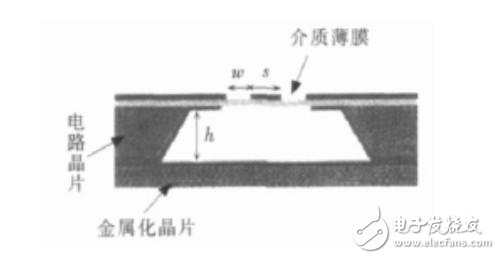
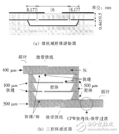
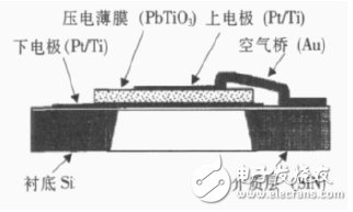
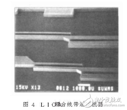
Filters, as a frequency-selective component, are used to suppress noise, select or limit the frequency range of RF/microwave signals, and play an important role in many RF/microwave applications. Conventional filters are bulky, costly to manufacture, and are not easily integrated with monolithic integrated circuits. They have large losses in the millimeter wave band, and MEMS technology generated by the fusion of microelectronics technology with mechanical and optical fields has been miniaturized. , diverse and integrated features. The combination of MEMS technology and RF technology, RF MEMS technology, offers new opportunities for the realization of a new generation of unique, high performance filters. At present, MEMS technology is applied to the design and manufacture of RF/microwave filters, resulting in high performance, small size, light weight, and low cost MEMS filters. MEMS RF/microwave filters can be designed with either lumped or distributed components, and can be implemented using a variety of structures such as microstrip lines, waveguide cavities, coplanar waveguides, and the like. Of course, they can also be implemented by a variety of manufacturing processes. 1. Silicon micro-machining MEMS filter The silicon micromachining technology realizes the three-dimensional structure of the device by etching the substrate silicon, and is often supplemented by Si-Si wafer bonding and Si-glass bonding. Due to the crystal orientation of single crystal silicon, a good anisotropic selective etching can be achieved by chemical methods (such as KOH), which is the basis of silicon micromachining. The silicon body micromachining technology can easily realize the three-dimensional processing of large longitudinal dimensions. A variety of MEMS filters have been implemented based on silicon micromachining technology. 1.1, thin film and microstrip line filter In order to reduce the loss from the substrate in the high frequency band, the cavity formed by the wet etching of silicon by ethylene diamine catechol using silicon micromachining technology realizes the dangling of the microstrip line, and SV Robertson et al. Band (94.7 GHz) coupled line bandpass filter. The geometry of the filter is fabricated on a transmission line supported by a film. As shown in Figure 1, the transmission line is equivalent to being suspended in an air medium. The dielectric loss is almost negligible and the radiation and dispersion parasitics are avoided. The filter has a passband insertion loss of 3.6 dB, where conductor loss is a major component of the overall component insertion loss. The relative bandwidth of the components is 6.1%. Similar to this technology, M. Chatras et al. implemented a high performance bandpass thin film filter with a center frequency of 30 GHz on a high resistance silicon substrate. The silicon under the film is selectively etched with tetramethyl ammonium hydroxide (TMAH). The filter has an insertion loss of only 1.8 dB and is easy to integrate into circuits that utilize flip chip technology. Figure 1 W-band coupled bandpass filter side view 1.2, micro-mechanical cavity resonators and filters The design of the filter can also be realized by using a cavity obtained by micromachining of the silicon body as a cavity. The X-band cavity resonator proposed by J. Papapolymerou et al. consists of an input-output microstrip line and a micromechanical cavity, and the cavity is coupled to the two microstrip lines through two slits (Fig. 2(a)). The two microstrip lines utilize a deposition of 7.5 μm thick gold to reduce losses; the thickness of the cavity metallization layer is 2 μm. Compared to other traditional metal rectangular and circular waveguide resonators, the resonator size is greatly reduced and has a high Q value (no load Q = 506, which is 4 times that of a conventional microstrip filter). L. Harle et al. implemented a bandpass filter with a center frequency of 10 GHz using a slot-coupled micromechanical cavity on silicon (Figure 2 (b)). The simulated bandwidth is 4% and the insertion loss is 0.9 dB at 10.2 GHz. The measured filter has a bandwidth of 3.7% and an insertion loss of 2 dB at 10.01 GHz. The difference in loss depends on the transition and line length of the microstrip transmission line. The overall size of the filter is 5 cm & TImes; 3 cm & TImes; 2 600 μm. The filter is characterized by low loss, narrow bandwidth, small size, and ease of monolithic integration, and has a strong power load capability due to surface current distribution over large conductor surfaces. Figure 2 Micromechanical cavity resonators and filters 1.3, thin film sound wave resonator and filter The concept of thin-film bulk acous TIcwave resonator (TFBAR) has been around since the 1960s, but its development has been subject to the level of microfabrication technology. With the rise of MEMS technology and advances in its processing technology, it is possible to produce TFBAR reliably and reproducibly, and also because of the ceramic or surface acoustic wave (SAW) filter commonly used in RF front-end modules. After the frequency band, the performance degradation due to the increase of the operating frequency, etc., many people began to research and develop TFBAR-based RF / microwave filters. The thin film bulk wave filter converts electrical energy into acoustic waves by the inverse piezoelectric effect of the piezoelectric film to form a resonance, which is superior to the SAW filter in terms of volume and power load. K. Misu et al. used a lead titanate material as a piezoelectric film to make a bulk acoustic wave filter, as shown in Figure 3. The two electrodes of the component are designed to be freely adjustable to produce oscillations at the desired frequency. The two electrodes also act as reflectors to counteract unwanted sound waves. The lower substrate material is etched by a silicon micromachining process to form a cavity, and the air-metal interface is used to obtain total reflection of the acoustic wave, thereby confining the acoustic wave to the piezoelectric film and the metal electrode. The resulting filter has an overall part size of 0.69 mm x 0.55 mm and a 3 dB bandwidth of 47 MHz at 1.5 GHz. YD Kim et al. [8] developed a filter using a ladder topology with this similar structure as the basic unit, with an insertion loss of only 2.8 dB at 5 GHz. Figure 3 film bulk acoustic wave filter For the silicon micromachining process, the chemical etching of silicon is limited by the crystal orientation, which further reduces the structural shape and size of the device. In addition, extensive etching of the substrate silicon also reduces the mechanical strength of the device. 2, LIGA planar transmission line and filter The word LIGA is derived from the acronyms of the German lithographie, galvanoformung and abformung, which represent the organic combination of deep lithography, electroplating and die casting. LIGA technology is an important means of achieving MEMS micromachining. It draws on the lithography technology in the planar IC process, but its aspect ratio for material processing is much larger than the planar process and thin film sub-micron lithography in standard IC production, enabling high aspect ratio 3D microstructures and processing. The thickness is also much larger than the typical value of the planar process of 2 μm. The process uses deep-radiation X-ray lithography to set the desired model on a thick layer of photoresist. X-ray is used as a light source for lithography. Its short wavelength and strong penetrating power for photoresist can achieve high resolution and high aspect ratio. Using LIGA technology, TL Willke et al. designed a coupled-line bandpass filter on a quartz substrate (Figure 4). Among them, the LIGA transmission line is 200 μm thick nickel and has two open ports! The /4 parallel line portion is used as a coupling unit with a coupling air gap aspect ratio greater than 6.75. There is a better coupling factor between the LIGA transmission line and the resonator compared to conventional thin metal. The bandpass filter has a minimum insertion loss of 14.5 dB at 14.6 GHz. Solar Panel,Glass Flexible Solar Panels,Thin Flexible Solar Panels,Monocrystalline Solar Panel Shengtian New Energy (Shenzhen) Co., Ltd. , https://www.stenergysolar.com