Xilinx Programmable Logic Device Design and Development (Basic) Serial 12: Spartan
The Spartan-6 device contains up to 6 CMTs and 12 PLLs. The main purpose of the PLL is as a frequency synthesizer, which produces a wider range of frequency outputs and has good filtering when connected to the DCM in the CMT.
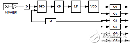
Figure 2-20 Spartan-6 PLL Functional Block Diagram
These include programmable counter D, Phase-Frequency Detector (PFD), Charge Pump (CP), Loop Filter (LF), and Voltage Controlled Oscillator (Voltage Controlled Oscillator). VCO), O0~O5 are 6 programmable counters.
It works by comparing the input clock to the phase and frequency of the feedback clock, and the resulting signal drives CP and LF. CP and LF generate a reference voltage for the VCO that affects the output frequency of the VCO. So how does the frequency of the VCO change? After the PFD completes the comparison of the two clocks, it generates the CP and LF drive signals, which determine whether the VCO should operate at a higher frequency or a lower frequency. When the VCO operating frequency is too high, the PFD triggers a falling signal, causing the control voltage to drop, thereby reducing the operating frequency of the VCO. When the VCO operating frequency is too low, the PFD triggers an up signal, causing the voltage to rise. The VCO generates a total of 8 output phases, and each output phase can be selected as the reference clock of the output counter, as shown in Figure 2-20. In addition, the PLL provides a dedicated counter M to control the feedback clock of the PLL for wide-area frequency synthesis. The six "O" counters can be programmed independently. For example, O0 can be programmed to perform a divide-by-2 operation while O1 is programmed to perform a divide-by-3 operation. The only restriction is that the VCO's operating frequency must be the same for all output counters because the VCO drives all counters. To use dedicated PLL routing resources, CLK_FEEDBACK must be set to CLKOUT0, using BUFPLL and BUFIO2FB as shown in Figure 2-21.
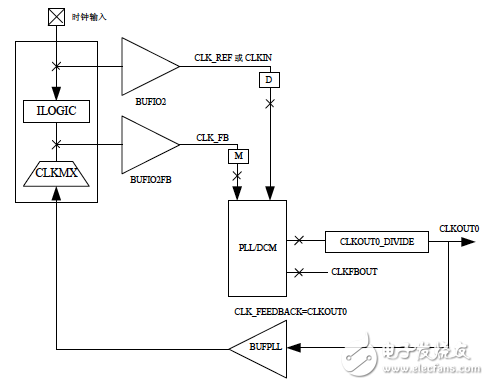
Figure 2-21 PLL with CLKOUT0 Feedback
When using the dedicated feedback path of CLKOUT0, the output counter CLKOUT0_DIVIDE will affect the VCO frequency, fVCO=FIN&TImes;M&TImes;CLKOUT0_DIVIDE/D.
Figure 2-22 shows two modules commonly used by the PLL, PLL_BASE and PLL_ADV. PLL_BASE allows the use of the most common functions of a separate PLL, including clock skew, frequency synthesis, coarse-grained phase shift, and duty cycle programming.
PLL_ADV has all PLL_BASE functions with more clock outputs.
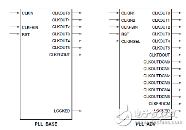
Figure 2-22 Primitives of the PLL
The Spartan-6 PLL is a mixed-signal module designed to support clock networks to skew SKEW, frequency synthesis, and jitter reduction. These three effects of the PLL will be discussed in detail next.
(1) The PLL skews the SKEW to the clock network.
In many cases, designers do not want delays in the clock network in their I/O timing budget. In fact, this problem can be solved with PLL/DLL because PLL/DLL has the function of compensating for the delay of the clock network. Of course, including the PLL in Spartan-6. A clock (usually CLKFBOUT or CLKOUT0) that matches the frequency of the reference clock CLKIN is connected to the BUFG and fed back to the CLKFB pin of the PLL. The rest of the output can still be used to synthesize the frequencies required by more users. In this way, all output clocks have a specified phase relationship with the reference clock. To accurately reduce skew due to clock input routing, it is recommended to use the BUFIO2FB buffer using the method shown in Figure 2-21.
(2) The PLL is used for frequency synthesis.
The PLL can also be used for frequency synthesis. In this application, the PLL cannot be used to skew the clock network, but to clock other modules. In this mode, the PLL feedback path should be set to internal feedback mode because all wiring is left as local wiring to minimize jitter. Figure 2-23 shows an example of configuring a PLL as a frequency synthesizer.
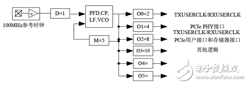
Figure 2-23 PLL for frequency synthesis only
In this example, the input is a 100MHz reference clock, setting M=5, D=1, the frequency of the VCO crystal can be 500MHz (100MHz & TImes; 5), 4 of the 6 PLL outputs are programmed to provide the following clock.
250MHz GTP transceiver clocks TXUSRCLK and RXUSRCLK.
125MHz PCI Express PHY clock.
62.5MHz PCI Express user interface and BRAM interface clock.
50MHz logic clock.
In this example, there is no phase relationship between the reference clock and the output clock, but a phase relationship is required between each output clock.
(3) The PLL is used as a jitter filter.
The PLL always reduces the jitter inherent in the reference clock. The PLL can be instantiated to filter out the jitter of the external clock before driving another logic block, including DCM. As a jitter filter, the PLL is typically simply viewed as a buffer that regenerates the input frequency on its output (eg, FIN = 100 MHz, FOUT = 100 MHz). In general, setting the BANDWIDTH property of the PLL to Low allows for strong jitter filtering, but note that setting BANDWIDTH to Low causes the static skew of the PLL to increase.
How to use PLL? There are usually the following methods.
The PLL Wizard in the ISE software can help generate various PLL parameters.
The PLL can be manually instantiated into a single component.
The PLL is merged with the IP core, which will contain and manage the PLL.
There are five application models for PLL, which are described below.
(1) The clock network is skewed.
I-Beam Inductors,Chip Inductors,Color Ring Inductor,R-Bar Inductors
Shenzhen Sichuangge Magneto-electric Co. , Ltd , https://www.scginductor.com