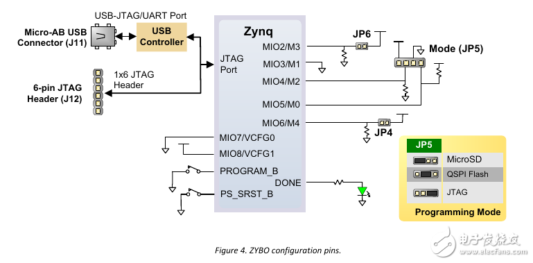
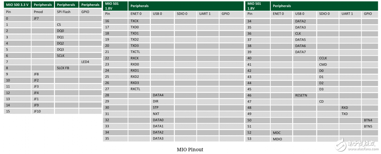
In order to learn RISC-V and experience the development platform of Xilinx, I recently started the Zybo Board, a development board with an FPGA and an ARM Cortex-A9 dual core. Before we start this, we need to have a little bit of information about this board and its periphery. To understand the periphery of the Zybo Board, the first thing to look at is the ZYBO FPGA Board Reference Manual provided by the developer DIGILENT. Let's take a look at some of the more important places! Basic hardware understanding Let's take a look at these peripheral modules. Power input (5V) The position of the control power input is on the header of JP7. We can select the power input we need by switching the jumper. When there is not much peripheral use, I will use USB (5V) directly. Current input. It should be noted that the Zybo Board only eats 5V power, so whether you use an external power supply (J15) or an external battery, you should first confirm whether your voltage is 5V (or lower), otherwise your The development board may burn out. After the power is plugged in, the power-on/off operation can be completed by switching the power switch (Power Switch, SW4). Zynq SOC We can divide the Zynq SoC into two blocks, the Processing System (PS) and the Programmable Logic (PL). Processing Syste (PS) is the ARM Cortex-A9. Part of the processor, Programmable Logic (PL) is the part of the FPGA. In the above block diagram, we have to pay attention to MIO (MulTIplexed I/O) and EMIO (Extended mulTIplexed I/O). In the Zynq 7000 series SoC, we have 54 MIOs available, and these MIOs are connected. The address is not visible in the Programmable Logic (PL). On the Zybo Board we have these places connected to MIO (MulTIplexed I/O) System startup process Because the Zynq 7000 series has built-in ARM CPU, the system startup process will be different compared with the traditional FPGA development board. The overall boot process can be divided into three phases: o Stage 0 If the BootROM is executed because the RESET button is pressed, the Zybo board selects the power-on state that was previously stored in the mode register instead of the current JP5 state. o Stage 1 When the Programmable Logic (PL) is set, the FSBL will load the program (ex: u-boot) and execute it. o Stage 2 Changing the boot mode We can switch the JP5 jumper to determine which way we want to load the first stage bootloader (FSBL). Bare Conductor
Bare conductor products including:
All Aluminum Conductor
All Aluminum Alloy Conductor
Aluminum Conductor Aluminum Alloy Reinforced
Aluminum Conductor Steel Reinforced
Aluminum Alloy Conductor Steel Reinforced
Aluminum Conductor Aluminum Clad Steel Reinforced
Thermal Resistant Aluminium Alloy Conductor Steel Reinforced
Galvanized Steel Wire
Aluminium Clad Steel Conductor
Copper Clad Steel Conductor
Steel Strand for Prestressed Concreter
Bare Copper Conductor
Tie Wire
OPGW
Bare Conductor,Aac Cable,Opgw Cable,Center Stainless Steel Tube Cable HENAN QIFAN ELECTRIC CO., LTD. , https://www.hnqifancable.com
The Zybo Board that gets the hand will look like this. We have these basic I/O modules, as well as the unmarked parts (Pmod), which can be extended. 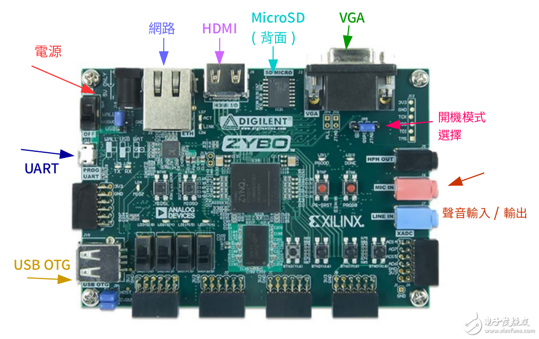
The Zybo Board allows three different types of power input modes, USB, external power supply (J15), and external battery. We can get general information about the power module from the Reference Manual. 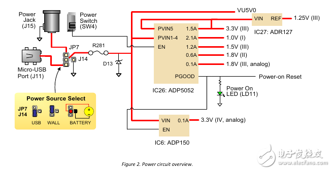
The Zybo Board core is the Xilinx Zynq-7000 series of Z-7010 ARM/FPGA SoC processors, an FPGA core that blends FPGAs with ARM Cortex-A9 processors. In the past, the FPGA development board needed to use the CPU to write only the soft core written in HDL language to the development board. This hybrid FPGA/ARM development board allows you to use ARM CPU for general purpose development. The special requirements are handled by FPGA processing/acceleration, which is a very interesting architecture. 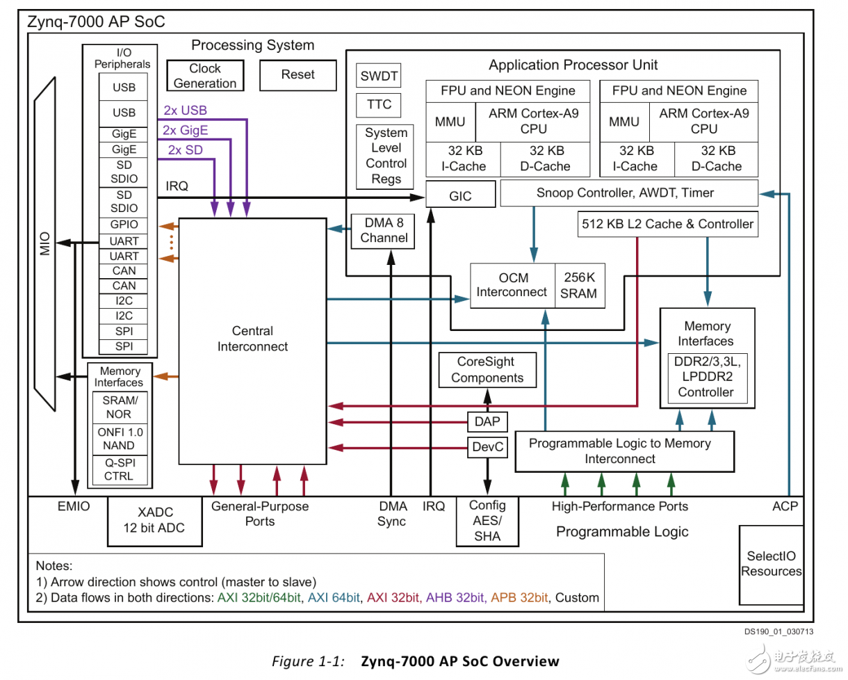
When the Zybo board power is turned on, CPU0 will execute the internal pre-burned program BootROM. This program will update the mode register according to the information set by JP5. Then the BootROM will pass the status register (mode register). The information is captured from the MicroSD, NOR Flash, JTAG and other locations to capture the Zynq Boot Image, and the first stage bootloader (FSBL) packaged in the Zynq Boot Image is copied to the internal 256KB of memory (On-Chip) Memory, OCM) Go, finally execute FSBL and move on to the next stage.
In this phase, the first stage bootloader (FSBL) initializes the peripheral settings of DDR memory, GPIO, etc., and then loads the bitstream stored in the Boot Image, which can be used by him. The program logic block (Programmable Logic, PL) is set.
The final snippet is the program loaded by the FSBL. These programs can be used to load Linux or other operating systems from a simple "Hello World" to a second-stage boot program like u-boot.