Design and Implementation of Parallel Computing Platform Based on FPGA and PCI Bus
Currently for various encryption algorithms. In addition to targeted cracking algorithms, the most basic idea is to match the exhaustive keys, often called brute force algorithms. Since the brute force algorithm contains a large number of keys, the traversal time exceeds the actually acceptable range. If the calculation speed is increased enough fast. This traversal algorithm has practical application prospects due to its simple structural design.
PCI bus (peripheral interconnect bus) has higher transfer rate (132MBps), support for 32-bit processor and DMA and plug and play compared with the traditional bus standard ISA bus (industry standard structure bus) It is used to replace the ISA bus and become the factual I/O bus standard for desktop computers. It has a wide range of applications on ordinary PCs and industrial PCs. The PCI bus provides a good way to meet the high-speed data transfer requirements in the card and system memory.
The PCI bus is a processor-independent local bus. Therefore, inserting an expansion board through the PCI bus and utilizing and improving the computing power and speed of large-scale digital signal processing by ordinary PCs and industrial computers is a very practical work. .
With the increasing application of digital technology, ASIC devices represented by field-programmable gate arrays (FPGAs) have rapidly spread and developed, and device integration and speed are increasing at a high speed. FPGAs combine the high logic density and high reliability of gate arrays with user-programmable features of programmable logic devices to reduce system design and maintenance risks, reduce product cost, and shorten design cycles. FPGAs have the following significant advantages over general-purpose CPUs:
(1) FPGAs generally have multiple adders and shifters, which are especially suitable for parallel processing of the same operations in multi-step algorithms. A general-purpose CPU can only provide limited multi-stage pipeline operations.
(2) Several algorithms can be integrated into one FPGA for parallel operation. A general purpose CPU can only be processed serially on one algorithm.
(3) Based on FPGA design, the board has low power consumption, small size and low cost, and is especially suitable for parallel connection of boards.
The system implementation of the PCI bus-based FPGA computing platform introduced in this paper: by inserting an extended PCI card on a PC, the algorithm is designed for parallel computing, and the processing speed of the large computing digital signal by the ordinary PC is improved. This design uses five FPGA chips and related peripheral chips to realize this parallel high-speed computing platform, and completes encryption and decryption of algorithms such as DES and MD5 on the platform. In this paper, the cryptography scheme based on the MD5 algorithm (the password verification of the Yahoo mailbox) is used to brute force, which verifies the feasibility of the system and the advantages of high speed and high cost performance.
1 system structure
The system uses ordinary PC or industrial computer for control, data stream download and result collection. The large amount of computational digital operations are performed in parallel in the FPGA using IP-CORE technology. The digital signal processing algorithm is designed as a unit module, and the layout and wiring are optimized according to the structure of the chip. The technology of the unit module reuse is called IP-CORE technology. In this system, the reusability of TP-CORE is utilized, and the allocation of data is scheduled through arbitration logic, thereby implementing parallel processing of the algorithm.
1.1 Hardware Structure
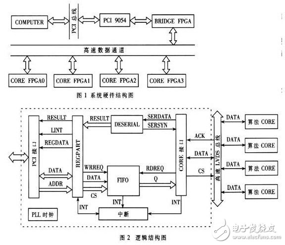
Five ALTERA company's STRATIX EP1Sl0 FPGA chips are used in the system, four of which are used as the carrier of the digital signal processing algorithm CORE (referred to as algorithm FPGA in the text); l is used as the bridge chip, loader and parallel bus ruling for connecting PC and computing CORE. And the carrier of arbitration logic such as interrupt judgment. The interface with the PCI bus uses the PCI9054 chip from PLX. The system hardware structure is shown in Figure 1.
1.2 Logical structure
The BRIDGE FPGA program adopts a top-down design method. Its logic structure is shown in Figure 2. It can be divided into the following parts according to functions: top-level module PCI_FPGA_PARALLEL; interface module PCI interface with PCI9054; data cache and arbitration part: data cache Module FIFO, register module regpart, data backhaul module deserial, internal bus arbitration, and flow control module CORE interface.
The PCI interface part realizes the interface timing with the PCI9054 chip, so that the multiplexed address and data are separated, and the address space selection and the enable signal are generated, which is convenient for the back end processing.
Arbitration logic:
(1) Realize reading and writing of data buffers and various registers in the address space, and perform corresponding operations (configuration, start, stop, reset, etc.) on the algorithm CORE and the bridge FPGA according to the contents of the configuration register.
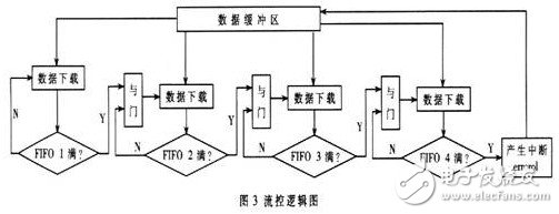
(2) Data flow control is performed using the buffer length and the queue length signals wrusedw, rdusedw, full, and empty of FIF0. When the data is downloaded by the PC, it first enters the buffer. Each algorithm CORE corresponds to a data downlink FIFO, and the current state of the FIFO determines whether to take the number from the buffer. The specific logical model is shown in Figure 3.
(3) The return result introduces a local interrupt mechanism. When a correct result is generated, or there is no correct result but the key match is completed, or the system is in an abnormal state, an interrupt signal is generated and the interrupt type register is filled in, and the cascading is generated to the PC. Interrupted. The interrupt decision is shown in Figure 4.

(4) Implement protocol logic with the algorithm core to control the downlink of various data streams and the return of results.
2 Introduction to MD5 algorithm
The MD5 (Message Digest 5) message digest algorithm is a widely used algorithm for extracting digital fingerprints. It was designed and invented by Rivent, one of the inventors of MIT cryptography experts and RSA algorithms. The MD5 algorithm structure is shown in Figure 5.
For any length of information input, MD5 will generate an output of 128 bits in length, which can be regarded as the "Message Digest" of the original input message.
Features of MD5:
(1) It is extremely unlikely that two different messages have the same message digest value.
(2) For a given message digest value, it is computationally impossible to find a message such that its message digest value is equal to a given message digest value.
(3) According to the abstract value of the message, it is extremely difficult to guess the original message.
The MD5 algorithm is widely used in network data integrity checking and various data encryption technologies.
The Yahoo mailbox crypto algorithm is based on two MD5 algorithms. The common algorithm steps are as follows:
Stepl: For a password field (for example: dfeag~hyt), encrypt it with MD5 algorithm: h=md5 (dfertgrhyt).
Step2: Convert the result of step1 to a hex value of 32Bytes: hex(h).
Step3: Simply cascade the result from step2 with a chanllenge value provided by yahoo: string=hex(h)+chanUenge
Step4: Perform the MD5 operation on the result of step3 again: hash=md5(strmg).
Since the actual Yahoo mailbox password generation parameters (such as the challenge code) are not obtained, this paper constructs a similar algorithm to test the performance of the system.
The test plan is as follows:
A known challenge value and a corresponding hash value are provided, and a suitable password is extracted from the provided dictionary, and the matching algorithm calculates that the corresponding hash value matches the provided hash value to verify the matched password. There are two ways to generate the key dictionary: artificially construct the dictionary and the system to add and exhaust the key.
3 measured performance analysis
In the actual system, the algorithm CORE operation clock is 20MHz, 64bit data width input; the multi-stage pipeline design and operation speed is the speed of the system running clock. In addition to the initial stage of the pipeline establishment process and the completion of the pipeline at the end of the operation, the operation speed can be regarded as 20MHz; the actual system is a parallel operation of four algorithms FPGA, the actual throughput is 4 & TImes; 20M & TImes; 16bit = 1.28Gb; Quartus 4.1 synthesis, the actual arbitration logic occupies 3,725 logical units. The integrated frequency is up to 156.2MHz, and the single algorithm logic occupies 7718 logic units, and the integrated frequency is up to 37.10MHz.
A typical ordinary PC fixed-point operation requires multiple instruction cycles, including instruction cycles such as fetching instructions, fetching data, calculating, and saving data. An x86 instruction cycle is composed of multiple CPU clock cycles, which greatly reduces the actual operation speed. Since a single CORE is operated by a 20MHz clock pipeline, which is equivalent to the operation speed of an ordinary PC, multiple CORE parallel operations can achieve parallel computing efficiency of multiple PCs.
Taking the key dictionary from the exhaustive generation of the FPGA can maximize the performance of the algorithm CORE. If the key dictionary is used to download from the PC, the actual rate is determined by the maximum PCI bus rate. However, since the dictionary can be artificially selected, the blindness of key selection is greatly reduced. The system is connected to the 32-bit, 32-MHz PCI bus on an ordinary PC, and the single-encryption CORE continuous operation (64 bit & TImes; 20 MHz) can satisfy the full-speed download of the PCI bus. If you use a 64bit, 66MHz PCI bus or PCI Express, you will further increase the actual throughput of the system.
This paper proposes an FPGA-based parallel processing structure suitable for large-scale digital signal processing. With the replaceability of CORE, different COREs can be designed for digital operations of different applications. The versatility of the system is very significant. Several PCI cards can be inserted simultaneously in one ordinary PC. Any algorithm FPGA on each card can provide comparable or more than one ordinary PC. For each additional algorithm FPGA, the power consumption is increased by no more than 10W under the premise of double the efficiency, and the volume is almost unchanged, and the cost is only one-fifth higher than that of the ordinary PC. therefore. The parallel structure proposed in this paper has a very high cost performance.
If the PCI bus interface module is integrated into the FPGA to replace the PCI9054 chip, the hardware cost will be further reduced and the complexity of the hardware design will be reduced. Because the actual operation speed is closely related to the parallelism and optimization of the algorithm, therefore, different applications are designed. The optimization of CORE and related algorithms is an important task to be carried out in the next step.
Soap Dispenser, also called soap dispenser and soap dispenser, is characterized by automatic and quantitative hand sanitizer. This product is widely used in public toilets. Avoid contact and use soap to clean your hands and other hygiene, which is very convenient and hygienic. In terms of function, the Sensor Soap Dispenser can be divided into two functions: with lock and without lock. It is more appropriate to choose a lockless soap dispenser in hotel rooms. Hotel toilets can be locked to prevent waste of soap. The size of the soap dispenser determines the amount of soap that can be filled, this can be based on the actual needs of the hotel, choose a suitable size product.
The Wall Mount Soap Dispenser generally includes a liquid tap fixed on the countertop, a soap bottle set under the countertop, a liquid discharge mechanism for pumping out the soap in the soap bottle, and a pressure button for driving the liquid discharge mechanism. Wait. Generally, the soap dispenser is matched with the sink and installed near the tap of the sink. When installing the soap dispenser, you need to check whether the sink has a soap dispenser hole, otherwise it cannot be installed.
There are many types of Touchless Soap Dispenser. There are also many colors of soap dispensers. Different colors of soap dispenser can be selected according to different places. The standard stainless steel color of soap dispenser can generally be divided into stainless steel bright color and stainless steel wire drawing color. The bathroom in five-star hotels chooses stainless steel bright color, and high-end clubs can choose stainless steel red.
Soap dispensers are mainly used in star hotels, restaurants, hotels, public places, hospitals, airports, home furnishings, pharmaceuticals, food, chemicals, electronics, high-end office buildings, large shopping malls, large entertainment venues, large banquet halls, hot spring resorts, kindergartens, For schools, banks, airport terminals, families, etc., it is your ideal choice for pursuing a noble and elegant life!

Soap Dispenser
Sensor Soap Dispenser,Touchless Soap Dispenser,Wall Mount Soap Dispenser,Refillable Soap Dispenser
Taishan Jie Da Electrical Co., Ltd , https://www.ts-jieda.com