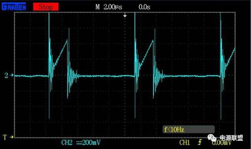
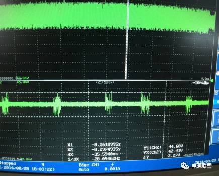
1. The low frequency ripple is related to the filter capacitor capacity of the output circuit. The capacity of the capacitor cannot be increased indefinitely, resulting in the residual of the output low frequency ripple. After the AC ripple is attenuated by the DC/DC converter, it appears as low-frequency noise at the output of the switching power supply. The size is determined by the ratio of the DC/DC converter and the gain of the control system. The ripple rejection of the current mode control DC/DC converter is slightly higher than that of the voltage type. However, the low frequency AC ripple at the output is still large. To achieve a low ripple output of the switching power supply, filtering must be applied to the low frequency power supply ripple. It can be eliminated by using pre-stage pre-regulation and increasing the DC/DC converter closed-loop gain. Several common methods of low frequency ripple suppression: a. Increase the inductance and capacitance parameters of the output low-frequency filter to reduce the low-frequency ripple to the required index. b. Adopt feedforward control method to reduce the low frequency ripple component. 2. The high-frequency ripple noise is derived from the high-frequency power switching circuit. In the circuit, the high-frequency switching of the input DC voltage is performed by the power device, and then the rectifier filter is implemented to achieve the regulated output, and the output terminal and the switch are operated. The high frequency ripple of the same frequency has its influence on the external circuit mainly related to the switching frequency of the switching power supply and the structure and parameters of the output filter. In the design, the operating frequency of the power converter is increased as much as possible, and the high frequency switching pattern can be reduced. Wave filtering requirements. The purpose of high-frequency ripple suppression is to provide a path for high-frequency ripple. The commonly used methods are as follows: a, improve the switching power supply operating frequency to improve the high frequency ripple frequency, which is conducive to suppressing the output high frequency ripple b. Increase the output high-frequency filter to suppress the output high-frequency ripple. C, using multi-stage filtering. 3. Since there is parasitic capacitance between the power device and the heat sink base plate and the original and secondary sides of the transformer, the wire has parasitic inductance. Therefore, when the rectangular wave voltage acts on the power device, the output terminal of the switching power supply will generate common mode ripple noise. . Reduce and control the parasitic capacitance between the power device, the transformer and the chassis ground, and add common mode rejection inductance and capacitance on the output side to reduce the common mode ripple noise of the output. Common ways to reduce the output common mode ripple noise: a, the output uses a specially designed EMI filter. b. Reduce the amplitude of the switch glitch. 4. The ultra-high frequency resonant noise is mainly derived from the diode junction capacitance of the high-frequency rectifier diode in reverse recovery, the resonance of the power device junction capacitance and the line parasitic inductance when the power device is switched, and the frequency is generally 1-10 MHz, and the soft recovery characteristic diode is selected. Measures such as small junction capacitance and reduced wiring length can reduce UHF resonance noise. Switching power supplies require closed-loop control of the output voltage, and improper design of the regulator parameters can also cause ripple. Entering the regulator loop through the feedback network as the output fluctuates may cause self-oscillation of the regulator, causing additional ripple. This ripple voltage generally has no fixed frequency. In the switching DC power supply, the output ripple is often caused by improper selection of the regulator parameters. This part of the ripple can be suppressed by the following methods: a. The compensation network of the regulator is added to the ground, and the compensation of the regulator can suppress the ripple increase caused by the self-excitation of the regulator. b. Reasonably select the open-loop amplification factor of the closed-loop regulator and the parameters of the closed-loop regulator. If the open-loop amplification factor is too large, it may cause oscillation or self-excitation of the regulator, so that the output grain content increases, and the open-loop amplification factor is too small. The output voltage stability is deteriorated and the ripple content is increased. Therefore, the open-loop amplification factor of the regulator and the parameters of the closed-loop regulator should be reasonably selected, and the adjustment should be made according to the load condition during debugging. c. No pure lag filtering link is added in the feedback channel. The delay lag is minimized. To increase the fastness and timeliness of the closed-loop regulation, it is beneficial to suppress the output voltage ripple.
The composite terminal is a typical representative of the connector (CONNECTOR), which is composed of a plug (female) and a socket (male) to realize the connection function. For the transfer of voltage, current and signal, this series is characterized by safe, reliable and stable contact, and is mainly used in electric power, communication, industrial control and other industries.
composite terminal block,component terminal block,composite terminal block adapter Sichuan Xinlian electronic science and technology Company , https://www.sztmlchs.com