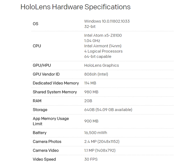
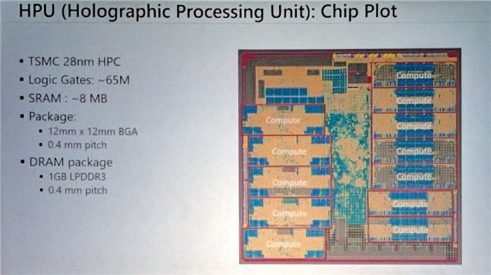
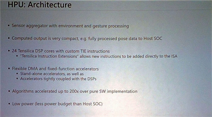
The Hot Chips conference in Silicon Valley was a lot of dry goods. In addition to the Tegra Parker car processor announced by NVIDIA, Microsoft also disclosed the Holographic Processing Unit, the secret chip in the Microsoft HoloLens MR helmet. In fact, the configuration of Microsoft HoloLens is public, we can see that it uses the Intel Atom x5-Z8100 CPU, 2GB RAM, 64GB ROM, 16500mWh and so on, but on the GPU/HPU, Microsoft has not announced its specific use. The model, on the information previously disclosed, only marked HoloLens Graphics. At the Hot Chips conference, Microsoft officially released the mysterious "HoloLens Graphics". It was named by Microsoft as the Holographic Processing Unit (HPU). It is a customized multi-DPS integrated chip using the TSMC 28nm HPC process, which consists of 24 Combining Tensilica DSPs, it can handle 1 trillion operations per second and integrates 8MB of SRAM cache and 1GB of DDR3 RAM. It is packaged in a BGA package and has a package area of ​​only 12x12mm. Compared to software-based solutions, its advantages are a 200x performance increase and only 10W of power consumption. Through the scalability of Tensilica DSP, Microsoft will add 10 special operating instructions designed to speed up the processing of HoloLens to improve the ability of the HPU to handle VR and AR data. At the same time, the HPU will perform pre-processing on the returned data for the Windows 10 system. The computational burden of the CPU (Intel Atom x5-Z8100). best dc current sensor,best current sensor,ac current sensor,battery current sensor Shanghai Zhilong Electronic Technology Co.,Ltd , https://www.zhilongsensor.com