Design and Implementation of ADSL Transceiver System-on-Chip Asymmetric digital subscriber loop (ADSL) is currently the most promising and competitive type of broadband access network technology [1]. Although some advanced countries in Europe and America have achieved success on the ADSL demonstration network, in the current Internet application environment, there are still obstacles to the widespread application of ADSL. The main reason is that the ADSL system technology is more complicated. The integrated circuit (IC) design method is used to integrate multiple chips into the system through the printed circuit board (PCB). The actual performance of the system is not ideal, and the production cost of the ADSL equipment is higher. Difficult to promote. The system-on-chip design method [2] [3] [4] organically integrates various subsystems on a chip, which can well overcome the system performance problems caused by the multi-chip integrated system, making ADSL truly a high-speed, Low-cost Internet high-speed access technology. This article introduces the system-on-chip design of the ADSL transceiver and gives a detailed description of the hardware implementation. The designed system on a chip (System on a Chip) chip is shown in Figure 1. Among them, the memory core uses NMI Electronics memory core, PCI uses Eureka Technology's PCI core, DSP core selects a company's DSP core, and the DSP algorithm is independently designed and developed. The MCU core completes the communication, control, and management functions with the DSP core, ATM framer core, and various interfaces, including the coordination and control of the PCI bus interface, USB interface, 10BASE-T interface, and internal bus. DSP core is dedicated to complete various core algorithms in transceiver equipment, including ADSL sub-channel division algorithm, DMT (discrete multi-tone modulation) sub-channel bit allocation algorithm, power adjustment, nonlinear echo cancellation algorithm, adaptive equalization algorithm, etc. ; Analog front-end AFE core completes A / D, D / A conversion, line drive and splitter functions; ATM framer core completes ATM frame header positioning and framing functions, and the logic circuit among them completes CRC encoding and decoding, scrambling and decoding , RS codec, interleaving and deinterleaving, and TCM codec; through the mode selection, the design can work in ATM and STM modes; the chip also provides a control channel (RS232 interface) to achieve system management, monitoring and Debugging function. Design features: (1) The analog front-end core is integrated with other cores, avoiding the need for at least three of the four power supplies common in linear drive devices, and achieving a high-efficiency, low-power design. (2) It can be directly used as a line card in the DSL access multiplexer at the central office to provide high-speed Internet access services. (3) Support all the latest ADSL standards, including ANSI T1.413 Issue 2, ITU G.992.1 and ITU G.992.2. It also provides the low overhead, fast start-up and retraining functions required for G.Lite operation. (4) Provide all functions of configuring and controlling ADSL lines through the control port, reducing the management burden of the host controller. 2 Typical circuit design and implementation in the chip 2.1 ATM framer design The ATM framer completes the user data interface function. The user data interface divides the received Utopia interface or STM interface data into a fast Utopia interface or STM interface. The user data interface is divided into two parts: the receiving direction and the sending direction. The sending direction is from the chip to the chip. The processed data includes ATM data (utopia interface) and STM data. It is composed of ADSL superframes and is divided into interleaved channels. And fast channel; the receiving direction is to send the data of the interleaved channel and the fast channel through the deframing and other transformations, which are also divided into utopia interface data and STM data. Its general structure is shown in Figure 2. 2.2 Digital interface design According to the requirements of the ADSL protocol, the digital interface mainly scrambles and FEC encodes the fast and interleaved data in the channel to form data that can be transmitted. The general block diagram is shown in Figure 3. In the sending direction, the data from the fast channel and the interleave channel from the user data interface are first subjected to CRC check, and then enter the deframing module, in this module, the super frame is decomposed into one by one data The frame is stored in the buffer. Then scramble the fast and interleave data separately. This scrambling is to scramble each data frame. The scrambled data enters the RS programming module and then enters the transmit FIFO. For Interleave data, the interleaving process is performed after the FIFO is sent out, and then the two types of data are compared and allocated, and each sub-channel is allocated a certain number of bits. Among). 2.3 DMT modulation circuit design DMT modulation is one of the important modules in the system-on-chip of ADSL transceiver. It mainly completes the modulation of data on each sub-channel. Its quality is directly related to the performance of ADSL transceiver chip. Most calculations in DMT are done by DSP, such as FFT / IFFT, FEQ, TEQ, constellation encoding and decoding, Trellis encoding and Viterbi decoding. The communication with DSP is mainly done through data and program address bus. The general block diagram of the DMT modulation module is shown in Figure 4. In the transmission direction, the data stream from the digital interface is already a bit allocation stream for each sub-channel. This data stream is constellated in the constellation encoding module to convert the bit stream signal in the frequency domain into the constellation plane in the time domain. Complex (X + iY) signal, then 2D QAM modulation. At this time, Trellis coding (four-dimensional lattice state modulation) can be selected to generate redundant bits to enhance the reliability of transmission. Then store the constellation encoded data in the transmit buffer. Due to channel distortion or other reasons, the data from the buffer does not match the frequency and phase of the master clock in frequency and phase. Therefore, in order to adjust this mismatch, the data from the buffer first undergoes frequency adjustment and gain fine-tuning (FTG). Frequency adjustment is to adjust the transmission frequency to ensure that the transmission frequency is consistent with the ideal frequency. FTG is to adjust the gain sparse on each subcarrier. Then enter the inverse fast Fourier transform (IFFT), the DMT symbol in the frequency domain is converted into a signal in the time domain, sent to the transmission buffer, and finally sent to the analog front-end interface. In the receiving direction, the data from the analog front-end interface is after time domain equalization (TEQ). These data first enter the receive buffer, and then enter the fast Fourier transform (FFT) to convert the time domain DMT signal into a frequency domain signal. (512 points), and then eliminate the corresponding interference in the frequency domain equalization (FEQ) and phase adjustment module, send it to the receiving buffer, and then perform constellation decoding to convert the complex point of the constellation plane into a bit stream. If the received data uses Trellis encoding, then the decoded data in the constellation will be sent to the data interface after passing through the Viterbi decoding module. The time pilot signal transmitted in the 64th sub-channel is transmitted and received through DPLL digital phase-locked loop to ensure that the sending and receiving clocks are consistent with the pilot signal. When the constellation is encoded and decoded, if the position of the constellation point of the pilot signal is found to be inconsistent with the ideal point position, it must be corrected by the DPLL and phase adjustment / frequency adjustment module. At the same time, the monitor can send the center off R_INT4 signal to the management and control interface. Communicate with internal ARM core through ASB. The functions of DPLL are: (1) The function of recovering the pilot signal in DPLL. In order to ensure that the sending and receiving clocks have a fixed phase relationship, the method of inserting pilots is used in ADSL to transmit and recover clock signals. The transmitter transmits the independent pilot signal on the 64th subchannel while sending data.The sampling clock frequency is 2208kHz, and the pilot signal frequency is 276kHz.After the pilot signal is restored, the sampling clock frequency is locked using a phase-locked loop To achieve clock recovery. (2) In the PLL, a clock source is used to generate the internal required clock. Among them, internal clocks include: CPU clock, DSP clock, clocks of various algorithms, etc. The frequency of the external reference crystal of the PLL phase-locked loop may be: 35.328MHz. In Trellis encoding and Viterbi decoding, there is a bit error counter connected to them respectively. When an error occurs, the bit error counter is incremented by 1 to a certain value, and the internal ARM core is notified by sending interrupt signals T_INT5 and R_INT5. 3 Difficulties in designing the system-on-a-chip of the asymmetric digital user loop transceiver 3.1 DSP algorithm design and implementation The DSP algorithm is the core of the ADSL transceiver SOC chip, and its performance directly affects the performance of the entire chip. However, the DSP technology involved in the ADSL transceiver is very complicated, which adds difficulty to the design. The design of the DSP algorithm must first establish a management model, based on the model for algorithm design, and then design the optimization model and optimize the algorithm based on it, so that the algorithm is accurate, stable, and can well meet the performance requirements. The next step is the hardware and software implementation and the collaborative design and verification of the two. Verification is to optimize the VLSI hardware and functional structure, execute the algorithm efficiently and quickly, and finally integrate the DSP system. In order to reduce power consumption and improve the efficiency of electronic devices, the analog front-end AFE and microcontroller MCU core are integrated together. When integrating mixed-signal cores on a digital chip, the lack of linear resistance is a major problem because continuous-time sequential filters require good controllability and linearity of the on-chip resistors. The current switch DAC also uses a linear resistor to convert the current into a voltage. Separating digital noise from analog noise is another issue, and a completely differential design with a high common mode rejection ratio (CMRR) and power supply rejection ratio must be used. 3.3 System verification issues As the complexity of system-on-chip (SOC) increases, the traditional method of using HDL software simulators for verification is no longer sufficient. It cannot provide the required performance to check the correctness of system functions. Moreover, the verification of the SOC chip requires the establishment of a model for the entire system. A lot of actual conditions should be added to the model to prove that the entire system and the chip are working properly. Therefore, a flexible modeling environment is needed to handle a large number of system-level solutions. The processing interface entry (TIP) can provide a high-speed link between the abstract layer software and the detailed hardware implementation, execute task software, verify system-level operations, and quickly discover problems in the design. 3.4 System testing issues The test technology of SOC chip is more difficult. SOC chip test equipment must be able to accurately detect both analog and digital circuits, and support scan detection and nested memory detection. The traditional detection method of adding test vectors to the input pins and then observing the results from the output pins is no longer applicable. Because the traditional method test vector set will be too large, and the execution time will be surprisingly long. 4 Design and implementation Using hardware and software co-simulation design, on the large-scale EDA simulation software Cadence's digital and analog hybrid design tool Spectra, the hardware description language Verilog is used to complete the design input, and then complete design synthesis, functional simulation, place and route, post-simulation and generate construction bitstream files . The above introduces the system-on-chip design of the ADSL transceiver, gives a detailed description of the corresponding hardware design, and describes the design features and difficulties. The selection of teaching projectors, with rich and bright colors, high-resolution projectors, and high-brightness laser light sources, can meet the needs of various large and medium-sized indoor teaching scenarios in schools, and provide teachers with good projection interactive teaching. best business projector,office presentation projector,good office projector,office classroom projector,4k teaching projector Shenzhen Happybate Trading Co.,LTD , https://www.happybateprojectors.com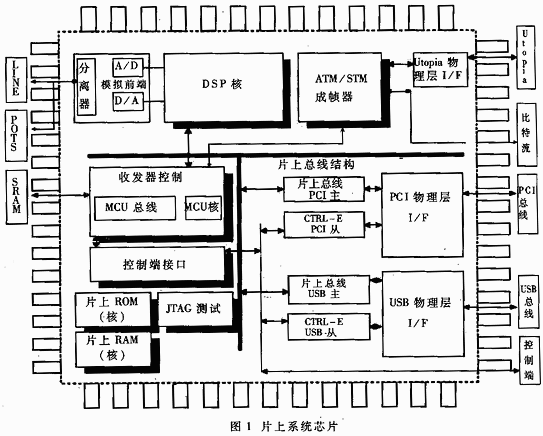
1 ADSL transceiver system-on-chip overall design 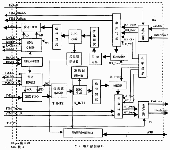
The STM interface includes STM_Data and STM_CLK two signals in the sending direction, and STM_Data and STM_CLK two signals in the receiving direction. In the sending direction, the STM signal is transmitted in a serial manner after parallel-to-serial conversion, SLT_Data0 transmits even-numbered bits, SLT_Data1 transmits odd-numbered bits, and then sends data into the channel classification according to the configuration of the external microprocessor (through the control interface) fast channel or interleave channel. In the receiving direction, the data from the fast channel and the interleave channel are combined into serial data in the channel combination. SLR_Data0 transmits the even-numbered bits, SLR_Data1 transmits the odd-numbered bits, and then is serially converted to the STM interface. Among them, the superframe indicator module mainly generates signals indicating the superframe (including the receiving and transmitting directions), VAL and REQ are valid signals for byte data, the Frame signal is the data superframe start signal, and the CLK signal is the superframe clock. According to the Utopia protocol, each byte of data in the Utopia interface is transmitted by one clock cycle, so it can take 53 clock cycles to transmit a cell. The synchronous clock signals in the sending direction and the receiving direction are sent by the ATM layer, and they can be regarded as asynchronous clocks. The data that enters the chip from the Utopia interface firstly decodes through the address, selects the port address for transmission, and then the transmission controller controls the data from the Utopia interface, stores them in the transmission buffer, and then goes to the cell rate interface controller. The function of the cell rate controller module is: When the cell rate sent by the ATM layer is less than the ADSL downlink transmission data rate, the cell rate controller inserts some empty cells to match the data rates of the two stems. The function of the HEC generation module: processing the HEC of the cell, and improving the cell delimitation ability when the sliding code appears. The processed cells are recorded in the received error counter and used for future performance monitoring. The function of the cell scrambling module: to prevent the same situation as the HEC in the cell load. The function of the frame adaptation module: organize the cell data stream into a data structure suitable for ADSL superframes. On the one hand, synchronization can be achieved by padding bytes LEX and AEX in ADSL. If the sending clock is a little faster, the fixed number of bytes will be used up, then LEX and AEX can be used to transfer the data. If the sending clock is a bit slower, the fixed number of bytes will not be used up. At this time, it can be expressed without a signal (ib) and processed by an external microprocessor. Another function of the frame adaptation module is that it can extract subsections such as aoc, eoc, and ib. The function of the parallel-to-serial conversion module: the data stream is converted into the channel classification module after parallel-to-serial conversion. The function of the channel classification module: combine odd and even serial data streams into a series of data streams, and send them into the fast channel or interleave channel according to the TxAdd signal of the Utopia interface or the configuration of the external microprocessor (registers in the control interface). It should be pointed out that the data flow in the receiving direction is opposite to the sending direction and will not be explained. 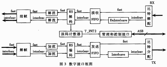
In the receiving direction, the data from the DMT modulation module enters bit de-matching, the Interleave data passes through the de_interleave module and then enters the receiving FIFO, and then enters the RS decoding module. For performance. After descrambling the data decoded from RS, it is sent to the framing module. In this module, each data frame is combined into a super frame, and then the data is CRC checked, and finally sent to the user data interface. 
3.2 Mixed design