Switching power supply secondary synchronous rectification unlock
1. When is the SR open and when is it turned off?
(In a word, first attach the BCD chip circuit diagram)
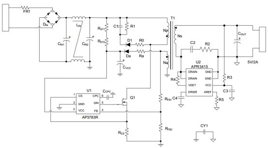
Figure 1
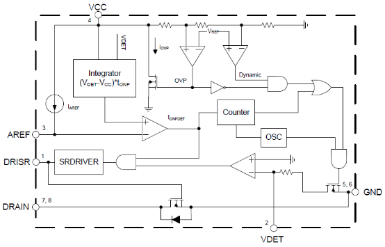
Figure 2
The APR3415 on the secondary side in Figure 1 is the protagonist of this chapter. Figure 2 shows the internal block diagram. It can be seen that the rectification MOS has been integrated into the chip (indicated by the red circle).
Then, when should it be turned on? The logic is actually quite clear: it should be turned off when the primary side is on, and it can be turned on when the secondary side is on. However, it's not directly controlled by the original control chip. How do we determine when to turn it on? We know that when the primary-side MOS Q1 turns on, based on the same-polarity end of the transformer (the black circle on T1), the secondary-side DRAIN pin becomes positive, so the rectification MOS must be turned off at that moment.
When the primary-side MOS turns from off to on, the polarity reverses. At this point, the secondary-side DRAIN pin becomes negative, allowing the rectification MOS to turn on, as shown in Figure 3.
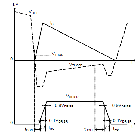
Figure 3
The VDET PIN detects the voltage of the DRAIN PIN through a resistor, so its potential matches that of the DRAIN PIN. When the DRAIN PIN voltage changes from positive to negative, it drops below a threshold voltage, VTHON (0V–1V). Once the VDET PIN detects this, it triggers an internal fixed delay TDON (70 ns), after which the MOS transistor is driven and starts conducting. Before the MOS turns on, the body diode continues to conduct, causing a relatively large negative voltage on the DRAIN PIN (as shown in the red circle). Once the MOS turns on, the current flows through the MOS instead of the body diode.
However, the secondary-side conduction current decreases linearly with the secondary-side voltage as the inductor demagnetizes. If the freewheeling current drops to zero, we still need to turn off the MOS. But when exactly? If the current isn’t fully stopped, the secondary-side capacitor may reverse charge the inductor, causing a backward current flow. If the primary side turns on while the secondary-side MOS is still on, this is called "common mode," which can cause serious issues. Therefore, timing the shutdown of the secondary-side MOS is crucial.
The ideal scenario is to turn off the MOS when the freewheeling current reaches zero, maximizing efficiency. But as the saying goes, “never make the last piece of copper,†so we prefer to turn it off just before the current approaches zero. This trade-off sacrifices a little efficiency for better reliability. The shutdown threshold is called VTHOFF (-20mV to -5mV). Once the VDET PIN crosses this threshold, the MOS is turned off after a fixed delay of TDOFF (100ns). After turning off, the body diode continues to conduct, resulting in a relatively large negative voltage (in the purple circle). If the primary-side voltage is sampled during this time, the output voltage may become unstable. The PSR primary-side chip’s voltage sampling mechanism is another topic worth discussing later.
Summary: The MOS turns on when the VDET PIN voltage is below VTHON (0V–1V), and turns off when it exceeds VTHOFF (-20mV to -5mV).
Two: How does the rectifier chip distinguish between primary-side conduction and ringing?
At first glance, it seems like the process is complete, but in reality, it's more complex than expected. When the rectification MOS turns on, there is a phenomenon called "ringing" on the DRAIN PIN. If the ringing amplitude is higher than VTHOFF, it could cause the MOS to shut down prematurely—often referred to as "cutting short the bloom." To address this, the chip includes a minimum ON time to prevent the MOS from turning off too early, ensuring it conducts long enough for the ringing to subside.
Additionally, if the VDET PIN voltage only dips below VTHON, what happens during the dead time before the secondary-side demagnetization is complete, before the primary side turns on? What causes the ringing? After demagnetization, the primary inductance LP and the stray capacitances of the primary MOS will oscillate briefly, creating a damped oscillation. This oscillation couples to the VDET PIN through the transformer, potentially triggering false shutdowns. To avoid this, the chip adds a condition to ensure the secondary-side synchronous rectification occurs only after the ringing has subsided.
To understand this better, let's look at Figure 4:
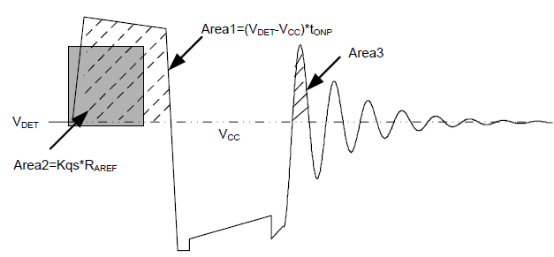
Figure 4
Figure 4 shows the VDET PIN voltage waveform over one cycle, including primary-side conduction, secondary-side demagnetization, and the dead time before the primary side turns on. Area1 corresponds to the primary-side on-time, where the voltage difference (Vdet-Vcc) is significant. Area3 represents the ringing during the dead time, which is much smaller in magnitude. By comparing the area under the curve, the chip can differentiate between the two.
This is achieved using an integrator circuit. The comparator Tonpdet (see the green circle in Figure 2) helps detect the primary-side on-time. The integrator accumulates the voltage over time, producing a rising voltage signal. The larger the input voltage and the longer the duration, the higher the output voltage. This allows the chip to distinguish between the large area (Area1) and the small area (Area3).
The integrator output is compared against a reference voltage set by the AREF PIN. If the integrator output exceeds this threshold, the MOS is turned on. Otherwise, it remains off. This ensures that the MOS only turns on when the correct conditions are met, avoiding false triggers caused by ringing or other transient signals.
The AREF PIN is connected to a resistor, generating a reference voltage. This voltage is used as a threshold to differentiate between the primary-side conduction and the ringing. By adjusting the resistor value, the threshold can be fine-tuned to match the system requirements.
It's also important to note that the AREF PIN is close to the VDET PIN, making it susceptible to noise. Adding a filter capacitor (typically 2.2nF) helps stabilize the threshold voltage. Too large a capacitor can slow down the response, leading to instability. Choosing the right value is essential for reliable operation.
Three: How to monitor the secondary-side voltage?
In many PSR chargers, the operation is typically PFM. At light or no load, the frequency drops significantly, sometimes to as low as 100Hz. The PSR sampling mechanism works by waiting for the secondary-side demagnetization before detecting the output voltage. This can lead to delayed responses when the load suddenly increases, causing a large drop in output voltage. The system may not react quickly enough, leading to instability.
To address this, the secondary-side rectifier chip uses the VCC pin to monitor the output voltage. If the voltage drops below a certain threshold, such as 5.25V, the chip can notify the primary-side controller to increase the pulse frequency. But how does the secondary-side chip communicate with the primary-side without an optocoupler or a separate transformer? The answer lies in the transformer itself. By turning on the secondary-side MOS, the output voltage is clamped, and the primary-side FB pin can sense this change through the auxiliary winding, triggering a pulse to restore energy.
However, turning on the MOS for too long can cause excessive energy absorption from the output capacitor, leading to reverse leakage tests. To avoid this, the chip integrates a high RDSON MOS (shown in the yellow circle in Figure 2), which is connected in series with a resistor to the VDET PIN. This allows the chip to send a small signal without overloading the system. The signal propagation is shown in Figure 7.
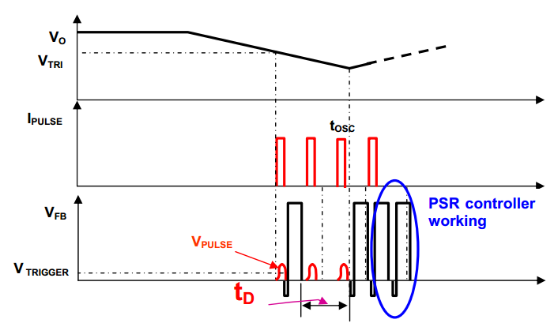
Figure 7
When the output voltage Vo drops below a threshold (Vtrigger), the secondary-side MOS turns on periodically (about 30μs) to generate a small current pulse. This pulse is coupled to the primary-side FB pin through the transformer. As long as one of these pulses exceeds the primary-side threshold (e.g., 83mV), the primary-side controller immediately pulses to restore energy. This method is efficient and avoids unnecessary power consumption.
However, during the secondary-side demagnetization, there may still be ringing on the FB pin. The primary-side needs to distinguish between the ringing and the actual pulse. This is a common challenge and will be discussed in more detail in future articles.
This monitoring mechanism also leads to another benefit: at very light loads or no load, the secondary-side can take full control, allowing the primary-side chip to enter sleep mode (turning off non-essential modules). Only the FB detection module remains active, reducing power consumption. When a pulse is detected, the primary-side wakes up, sends a small pulse to transfer energy, and then returns to sleep. This ensures stable output even without a dummy load, minimizing standby power consumption.
However, the primary-side VCC capacitor continues to discharge. If the output voltage remains stable and doesn't drop below Vtrigger, the VCC voltage will eventually fall below the UVLO threshold, triggering a restart. To prevent this, the chip forces a wake-up pulse every 30ms, regardless of the load. This ensures the VCC capacitor stays charged, preventing unexpected restarts.
Finally, during load transitions, the output voltage may overshoot. To handle this, the chip includes a built-in MOS that bleeds excess energy from the output capacitor. When the voltage exceeds a threshold (Vdis, e.g., 5.35V), the VCC pin pulls 3mA of current. If this isn't enough, a stronger bleed (100mA) is activated at a higher threshold (Vovp, e.g., 5.8V). This prevents overshoot and stabilizes the output voltage effectively.
By the way, if the overshoot exceeds Vovp, the secondary-side chip stops sending pulses to the primary side. Why? Because the secondary-side voltage is already high, and adding more energy would only worsen the situation. If the output voltage drops below specification after a full-load cut, it could be due to the secondary-side being in a high-energy state while the primary-side VCC capacitor is low. Without a pulse to wake it up, the primary-side may trigger UVLO, leading to further instability.
Figure 8 provides a more intuitive understanding of the entire process described above (Von is the chip's working voltage, approximately 3V):
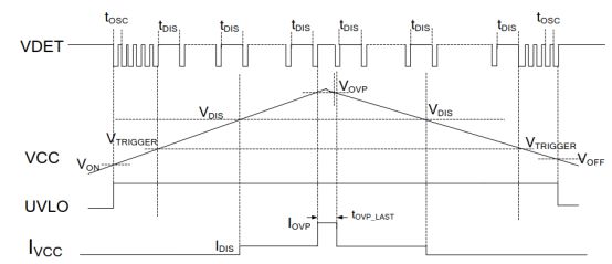
Figure 8
4D Laser Level,Laser Level Standard,Wall Mount Laser Level,Multiple Laser Level
Guangdong Tumtec Communication Technology Co., Ltd , https://www.gdtumtec.com