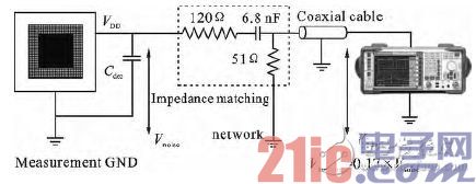
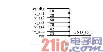
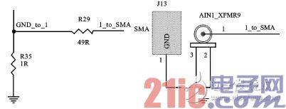
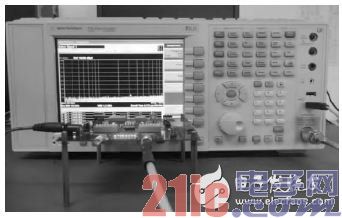
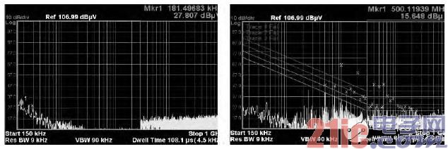
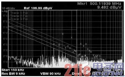
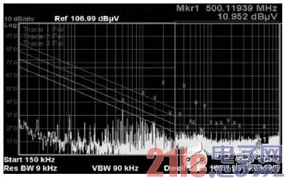
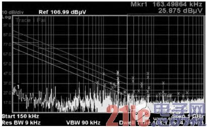
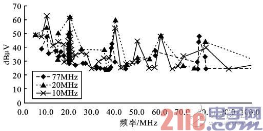
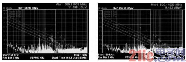
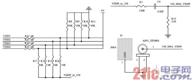
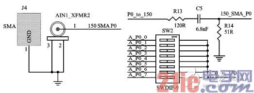
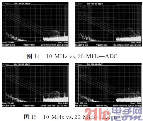
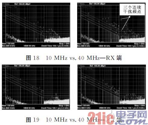
1 Introduction This article refers to the address: http:// As the integration of integrated circuits increases, more and more components are integrated into the chip, the circuit functions become complicated, and the operating voltage is also reduced. When the signal or noise generated in one or more circuits interferes with the operation of another circuit in the same chip, an on-chip EMC problem occurs, the most common being SSN (Simultaneous Switch Noise) and Crosstalk, which will affect the normal operation of the chip. Since the integrated circuit operates through high-speed pulsed digital signals, the higher the operating frequency, the wider the spectrum of electromagnetic interference, and the more likely it is to cause electromagnetic compatibility problems with external radiation. Based on the above situation, the electromagnetic interference (EMI) and immunity (EMS) problems of the integrated circuit itself have become the subject of attention in the design and manufacture of integrated circuits. Integrated circuit electromagnetic compatibility involves not only the design and test methods of electromagnetic interference and immunity of integrated circuits, but also the integration with the application of integrated circuits. For the automotive electronics field, the mandatory standards for electromagnetic compatibility requirements at the vehicle-level and component-level levels, combined with the design of integrated circuits, will make it easier for circuits to design end products that meet the standards. As the most critical unit in the electronic control system - the microcontroller (MCU), its EMC performance directly affects the control functions of each module and system. In this paper, the anti-EMI design method is adopted in the automotive electronic MCU, and the electromagnetic interference test of the automotive electronic MCU is carried out according to the IEC61967 conduction test standard. 2 Automotive electronic MCU design method The following describes the possible design methods used in automotive electronic MCUs and several other anti-EMI design techniques. 2.1 Clock circuit design Since the clock signals generated by the clock circuit are generally periodic signals, the spectrum is discrete, and the energy of the discrete spectrum is concentrated at a limited frequency. Moreover, since the clock signals of various parts in the system are usually obtained by frequency division and frequency multiplication of the same clock, their spectral lines are also multiplied, and overlap to increase the amplitude of the radiation. Therefore, the clock circuit is a very large one. Source of pollution. For the automotive digital MCU digital front-end design, the method of gated clock is improved in terms of anti-EMI. Any clock should be turned off when not needed, reducing the electromagnetic emissions caused by the operating clock. According to the design requirements of the chip system of A8128 (model of automotive electronic MCU), four working modes of Run, Idle, Stop and Debug are adopted, and the system clock and peripheral module clock are appropriately gated in each working mode. In addition, there are several anti-EMI design methods that are common in clocks, including: 1 reduce the working frequency The MCU's operating clock should be set to the lowest frequency required to meet performance requirements. It can be seen from the following test results that the operating frequency of an MCU is changed from 80MHz to 10MHz, which can cause the interference peak in the spectrum wide frequency range to generate tens of dBμV attenuation, and can effectively reduce power consumption. 2 asynchronous design The asynchronous circuit operates without locking a natural frequency, and the electromagnetic radiation is widely distributed over a wide range without being concentrated in a specific narrowband spectrum. This key essential feature determines that even if an asynchronous circuit uses a large number of active gates, it produces electromagnetic emissions that are smaller than synchronous circuits. 3 spread spectrum The spread spectrum clock is a technique that reduces the measurement of radiation. This technique modulates the clock frequency by 1% to 2%, spreads the harmonic components, and has a lower peak in the CISPR16 or FCC emission test, but this is not true. Reduce the instantaneous transmit power. Therefore, the same interference may still occur for some fast reaction devices. Spread spectrum clocks cannot be used in demanding time communication networks such as FDD, Ethernet, fiber, and more. 2.2 IO port design In the design of the input and output ports of automotive electronic MCUs, anti-EMI solutions have also been added, including slew rate control and drive strength control methods. By introducing a configurable toggle rate and drive strength register on all common P ports, the corresponding function is turned on when needed. The flip rate has two options: on and off. When turned on, it can effectively smooth the rising edge or falling edge, reduce the transient current, and thus control the electromagnetic interference intensity generated by the chip. The driving strength has two choices: strong driving current and weak driving current. When the working driving strength can be satisfied, selecting weak current driving will better control electromagnetic interference. In addition, based on the GSMC 180nm process library, selecting IO with Schmitt triggering characteristics can effectively smooth the spikes or noise signals brought in the input signal, which helps the electromagnetic immunity of the chip. 3 Automotive Electronics MCU Test Solution The IEC61967 standard is a standard for electromagnetic emissions from integrated circuits developed by the International Electrotechnical Commission for electromagnetic emission testing of integrated circuits with frequencies from 150 kHz to 1 GHz. The standard involves two types of test methods: radiation and conduction. Since the electromagnetic interference of the conduction mode has a greater impact on the application of the chip, the test is selected by the direct coupling method of IEC61967-4. The method is further divided into a 1Ω test method and a 150Ω test method. The 1Ω test method is used to test the total interference current on the ground pin, and the 150Ω test method is used to test the interference voltage of the output port. In the test, it is necessary to connect a current probe with a series resistance of 1 Ω in the circuit to be tested (the probe is a 1 Ω test network, which has been integrated between the chip ground of the EMC test board and the ground plane of the PCB), 49Ω series connection Placement To form a 50Ω match, the receiver measures the RF voltage generated by the RF current flowing through the resistor. The measured voltage should be the sum of all the RF currents flowing back to the IC on the current probe. The voltage value can be converted to the current flowing through the probe. The test environment diagram is shown in Figure 1. Figure 1 1Ω test environment In the 150Ω test, the pins of the integrated circuit are connected to the test receiver through a standard-matched matching network. The 150Ω probe (the probe is a 150Ω test network, already integrated on the EMC test board) can measure the SSN at the input and output ports. Conducted interference on the two types of pins and the power supply. The voltage measured by the receiver can be converted into the noise voltage amplitude by calculation. The test environment diagram is shown in Figure 2. Figure 2 150Ω test environment The following are 1Ω and 150Ω test steps for EMI, including pre-test preparation and test data analysis. 3.1 Equipment work before testing 1 ambient temperature The experiment was concentrated in the evening, and the site temperature was controlled within the range of 23±2 °C, which met the standard requirements. 2 ambient noise level The DUT (device under test) is fixed on the test bench and is in a power-off state, and the residual noise is measured by the EMI receiver. The ambient noise level of this test is within acceptable test requirements. See Figure 6 for details. 3 other environmental conditions All other environmental conditions that may affect the test results, such as ambient humidity. The relative humidity measured in this experiment was about 45% RH. 4 Confirm the working status Power the DUT and check that the IC is in normal working condition while maintaining the surrounding test conditions during the experiment. 3.2 1Ω test (1) Connect one end of the SMA cable to the test board and the other end to the receiver (Agilent N9030, built-in N141A EMC test software), set the measurement frequency range of the EMI receiver to 150kHz to 1GHz, according to the standard pair test operation The requirements are divided into two segments: 150 kHz to 30 MHz (RBW is 9 kHz) and 30 MHz to 1 GHz (RBW is 120 kHz). In the test chart below, the green border range is 150 kHz to 30 MHz, and the range is 30 MHz to 1 GHz. Combined with the characteristics of the automotive electronic MCU port and the standard requirements, the grounding port is connected to the 1 Ω network, and then connected to the SMA port to introduce an EMI receiver for monitoring. The schematic diagram is shown in Figure 3 and Figure 4. Figure 3 chip ground network pin Figure 4 1Ω network (2) Select the factors that may affect the EMC characteristics, test the electromagnetic interference size values ​​at 10MHz, 20MHz and 77MHz respectively on the clock, and select the analog-to-digital conversion program ADC on the test function; (3) Measure the interference that may occur in each spectrum, extract the envelope value of each harmonic, and the voltage of the receiver can be converted into the current flowing through the probe. The test instrument and the EMC test board are shown in Figure 5; Figure 5 actual test environment (4) Multiple measurements are taken at each frequency point to eliminate interference from accidental factors. The following is a description of each test case; The 1 clock uses an external crystal oscillator of 10MHz, and the program in the SRAM is programmed as an ADC. The left side of Figure 6 shows the ambient noise signal when it is not powered, and the right side is the measurement result of the power-on but not running program. Figure 6 Power off vs. power on By comparison, it can be concluded that the interference intensity becomes larger in the entire spectrum range after power-on, and the fixed period of the clock will concentrate the electromagnetic radiation in a narrow spectral range around the clock fundamental and harmonics. According to the Fourier series expansion formula, it can be concluded that the interference value is higher at the frequency point at the clock multiplier, so the phenomenon at the 10MHz, 20MHz and other multiplication points is more obvious. 2 For further comparison, run the ADC program and test it under the 10MHz, 20MHz and 77MHz clocks respectively, and compare the total interference current of different clock ground pins. The test results are shown in Figure 7, Figure 8, and Figure 9. Figure 7 10MHz-ADC test chart Figure 8 20MHz-ADC test chart Figure 9 77MHz-ADC test chart Figure 10 10/20/77MHz—ADC test data Fig. 7, Fig. 8, and Fig. 9 are test charts of 10 MHz, 20 MHz, and 77 MHz, respectively, and Fig. 10 is data after sorting. By comparison, it can be concluded that the spectrum is roughly concentrated within 100 MHz, and the interference value is the largest at the main frequency point of the corresponding working clock, and the interference value near the corresponding multiplication point (such as 40 MHz, 60 MHz, etc.) in the case of 10 MHz and 20 MHz. More concentrated. The extracted data yields a peak point of 9.999 MHz (62.643 dBμV) at 10 MHz, a peak point of 20.002 MHz (61.692 dBμV) at 20 MHz, and a peak point of 19.264 MHz (48.049 dBμV) and 77.042 MHz (47.316 dBμV) at 77 MHz. It can be seen that the interference intensity and density at 77MHz are weaker than 20MHz, which may be due to the fact that 77MHz is the limit clock for MCU operation, and the performance is affected to some extent, resulting in different test results. 3 Since the working clock of the automotive electronic MCU can select the external crystal or the internal PLL multiplier, it is necessary to test the two cases separately in order to compare whether there is a difference. The test results after running the ADC program are shown in Figure 11. Figure 11 PLL vs. External Crystal (10MHz) It can be seen from Fig. 11 that the distribution of peak points in the spectrum range is almost the same, and there is no significant difference in the whole spectrum range. The results measured by the MCU through external crystal oscillator or PLL multiplication are basically the same, and the clock source is selected. Does not affect the electromagnetic interference strength of the chip. 3.3 150Ω test (1) Step 1 of the device device connected to the same 1 Ω test method; (2) According to the type of chip power supply, the power supply is divided into 4 channels, which are VDD1 (5V power supply signal for digital IO supply), VDD2 (5V voltage for LDO for ADC and PLL), and VDD3 (5V voltage input for digital logic LDO). ) and VDD4 (Flash 5V voltage input). The interference noise of each power supply can be separately captured, and the connection mode is the same as that of step 1 of the 1Ω test method, as shown in FIG. 12; Figure 12 VDD Connection 150Ω Network 145 (3) According to the application characteristics of automotive electronic MCU, select the most typical PWM and CAN programs. In order to facilitate the separate measurement of many pins in the future, P0, P1, P2 (P3 does not involve peripheral function multiplexing) ports total 24 The pins are switched and controlled, and then connected to the EMI receiver through a 150Ω coupling network. Figure 13 is the circuit schematic of the P0 port. The schematic diagrams of P1 and P2 are the same as P0. Figure 13 IO-P0 connects to a 150Ω network (4) Repeat the test several times to get more test samples. After finishing, the following is a description of each test situation. 1 From the power port results, the difference is very small, the following VDD1 as an example for analysis and description. The VDD1 test selects the ADC and counter (digital counter) program to compare whether different classes of programs have an impact on the digital power supply. The test results are shown in Figure 14 and Figure 15. Comparing the 10MHz and 20MHz clocks, the maximum peak value of the ADC is 35.827dBμV and 43.517dBμV, respectively; the highest peak of the counter is 35.899dBμV and 43.271dBμV. It can be concluded that the higher the frequency, the greater the interference intensity. But in terms of horizontal comparison of the two types of procedures, the results are basically the same. In addition, it is also found that the interference spectrum is concentrated in two places of 60~300MHz and 550~650MHz. It can be seen that the interference at the power supply is obvious near the high frequency. 2PWM function test In the dual channel mode, the measured emission intensity at the corresponding P port pin is tested under different duty cycles and cycle sizes. The test results are shown in Figure 16 and Figure 17. The degree of influence of the clock on electromagnetic interference can be seen from the interference density in Figure 16. In Figure 17, because the period and duty are long, the test results are not much different. At this time, the clock frequency becomes a secondary factor, and the main factor depends on the length of the high-low level change period at the output pin. 3CAN function test Run the Loopback program and compare it at different clock frequencies. The test results are shown in Figure 18 and Figure 19. As seen from Figs. 16-19, as the clock frequency becomes larger, the conducted radiation intensity of the TX and RX ports also becomes larger. For the RX port, the interference density near the 10/40MHz frequency is relatively large, and the phenomenon is more obvious at 40MHz, capturing three consecutive frequency points (labeled on the right side of Figure 18), respectively 39.060 MHz (71.063dBμV), 39.360MHz (67.447dBμV), 40.020MHz (39.171dBμV), the peak value of both clocks is between 70~85dBμV, but generally below 10MHz, it should be affected by a certain frequency point of low frequency. For the TX port, the interference density near the 10/40MHz frequency is not as obvious as RX, and the peak value is also between 70~85dBμV, and occurs below 10MHz, which is similar to the characteristics of RX. 4 test results analysis From the test data results can summarize the following points: 1 At the clock frequency, from 10 MHz to 40 MHz, 77 MHz, the interference intensity or density will increase as a whole, which can be a small spectrum or the entire spectrum, which is more related to the test object. It is not difficult to find out because the clock signals generated by the clock circuit are generally periodic signals, the spectrum of which is discrete, the energy of the discrete spectrum is concentrated on a limited frequency, and the clock signals of various parts of the system are usually divided by the same clock. The frequency and frequency are obtained, and their spectral lines are also multiplied, which will overlap and increase the amplitude of the radiation. 2 In the program programming mode, the results measured by the external crystal oscillator or PLL multiplier are basically the same, there is no significant difference in the whole spectrum range, and the clock source selection will not affect the electromagnetic interference intensity of the chip. 3 From the VDD1 test results, in addition to the higher the frequency, the greater the interference intensity, it is also found that the spectrum range of interference occurs at 60~300MHz and 550~650MHz respectively, and the interference at the power supply is near the high frequency. More obvious. 4 For the PWM function, by configuring the output waveform period and duty cycle size, the electromagnetic interference intensity generated at different clocks will be different. Since the register in the dual channel mode is 16bit (the original single channel mode is 8bit), the cycle and duty cycle configurable values ​​become larger, and the high and low turnover periods at the PWM wave output pin depend on the period and duty cycle. The setting, the relationship with the clock has become so tight before, the clock has become a secondary factor. Therefore, it is recommended to increase the cycle and duty cycle values ​​as much as possible when using the PWM function under the premise of meeting the functional requirements, which will improve the EMC performance. 5 For the CAN bus, through the 10 MHz and 40MHz clock comparison, when the clock operating frequency is reasonably reduced, the interference value in a large spectrum range will be reduced, and the impact of EMI is better controlled as a whole. 5 Conclusion For the microelectronics industry, the design and testing of chip-level electromagnetic compatibility has become a very important topic. In fact, if you do not conduct in-depth research on the electromagnetic radiation and immunity of integrated circuits, it is difficult to meet the needs of electromagnetic compatibility of electronic equipment. This paper indirectly proves the necessity and importance of the design method by introducing the design method and further summarizing the factors and causes that affect the electromagnetic emission through the test scheme.
Reel with solid flanges, turned on the drum and in the central bore. The available sizes are as per DIN 46395 / 46397 specifications or as indicated by the Customer, for a normal use up to 1400 mm of flange diameter.
Indicated for metallic wires. To be used on a wiredrawing, stranding or rope-making machine. It withstands annealing treatment.
Flat Wire Spool, Panel High-speed Spools, Empty Spool, Cable Spools NINGBO BEILUN TIAOYUE MACHINE CO., LTD. , https://www.spool-manufacturer.com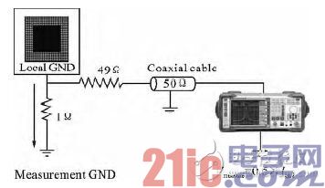

Serial Number
Specification Model
Lateral Plate Diameter D1
Major Diameter D2
Axle Hole Diameter D4
Carrying Hole Diameter D5
Center Distance E of Axle Hole and Carrying Hole
External Width L1
Internal Width L2
Remarks
1
285
285
130
165
127
18
180
260
240
Thin Extend Shaft
2
300
300
130
165
127
18
180
270
250
Thin Extend Shaft
3
335
335
165
217
127
18
180
270
250
Thin Extend Shaft
4
400
400
217
270
125
127
18
100
270
250
Middle Extend Shaft
5
500
500
217
270
125
127
22
130
320
300
Middle Extend Shaft
6
630
630
350
420
125
127
28
200
430
400
Twist Extend Shaft
7
300
300
130
165
56
8
100
290
270
Twist Extend Shaft
8
335
335
130
165
56
8
100
290
270
Twist Extend Shaft
9
400
400
165
217
70
16
170
270
250
Extend Shaft
10
500
500
217
270
80
16
100
320
300
Extend Shaft
11
560
560
270
295
80
18
120
355
329
Extend Shaft
12
610
610
270
320
80
22
170
360
336
Extend Shaft
13
630
630
355
450
125
127
28
200
360
336
Extend Shaft
14
710
710
400
500
125
127
28
100
530
450
Extend Shaft
15
800
800
450
560
125
127
28
100
600
500
Extend Shaft
