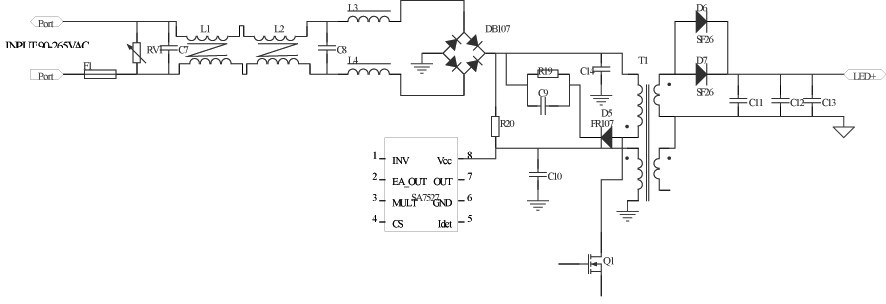
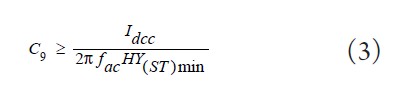
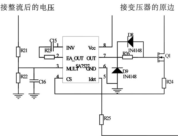
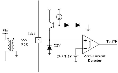
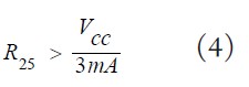
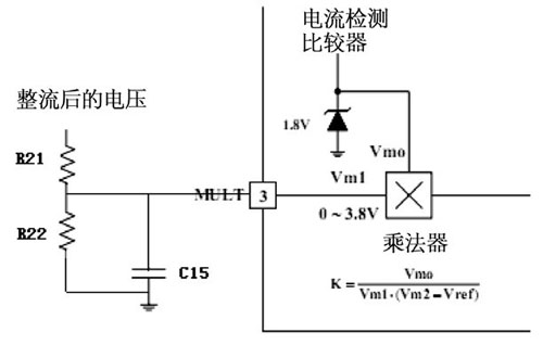
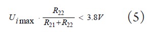
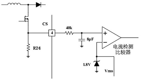
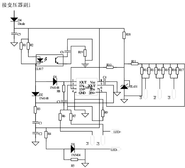
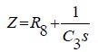
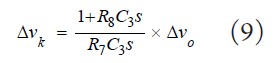
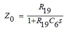
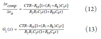
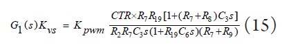
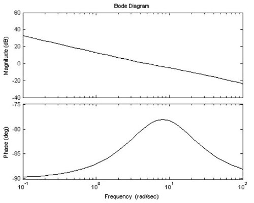
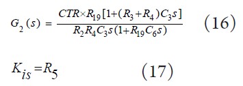
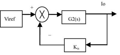
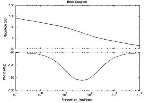
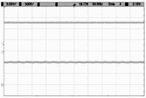
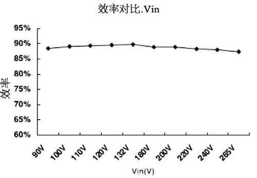
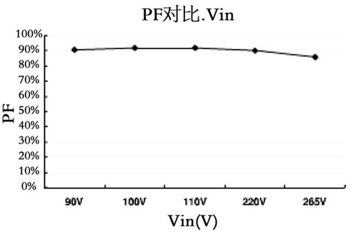
Abstract: This paper uses the SA7527 chip to design an LED fluorescent lamp driving circuit, which analyzes the various parts of the circuit. The topology of the circuit is a flyback converter, and the TL431, a dual-operational amplifier LM358 and an optocoupler EL817, are used to form a closed-loop feedback to achieve a constant current and constant voltage output. The circuit has the advantages of simple operation, wide input voltage range, low cost, good performance, stable and reliable operation. With the development of society, people are increasingly promoting green lighting. LED fluorescent lamps are widely used as one of them. LED fluorescent lamps have the characteristics of energy saving, long life and good applicability compared with ordinary fluorescent lamps, because of the volume of a single LED. Small, can be made into any shape, with short response time, environmental protection, no harmful metals, easy recycling of waste materials, brilliant colors, pure color and other advantages. In this paper, an LED fluorescent lamp driving circuit designed by SA7527 has better stability and reliability. It can not only reduce the cost of fluorescent lamps, improve its conversion efficiency, but also achieve constant current and constant voltage output, and can drive LEDs with different powers. First, the circuit design 1. Circuit composition The whole circuit is composed of anti-surge protection, EMI filtering, full-bridge rectification, flyback converter, PWMLED drive controller and closed-loop feedback circuit, as shown in Figure 1. Figure 1 Block diagram of LED driver circuit based on SA7527 2. Main circuit analysis The main circuit is shown in Figure 2. From the AC220V, the AC mains inlet is connected with a fuse F1 and a surge-resistant varistor RV1. The fuse acts as an overcurrent protection for the line input circuit. The varistor RV1 is used to suppress the instantaneous high voltage from the grid. Protect the safety of the input line, followed by the EMI filter, L1, L2, C1 are common mode filters, L3, L4, C2 are differential mode filters, DB107 is a full bridge rectifier circuit, C13 is a capacitor filter, rectified The post voltage (current) is still pulsed DC. In order to reduce fluctuations, a filter is usually added. The RCD buffer circuit consisting of R19, C8, and D5 is to prevent the power tube Q1 from withstanding a large back pressure during the turn-off process. The diode of the buffer circuit generally selects a fast recovery diode. The output filters C10, C11, and C12 are connected in parallel to reduce voltage ripple. The characteristics of this circuit: (1) wide voltage input range; (2) constant current / constant voltage characteristics; (3) output feedback sampling composed of LM358 and constant current / constant voltage control circuit, low cost, high control precision, debugging Simple; (4) This circuit can drive LEDs of different powers. 3. Start circuit design The startup circuit is shown in Figure 2. In order to make the circuit start normally, a starting resistor R20 should be connected between the transformer primary coil rectified by the rectifier bridge and the power supply terminal 8 of the SA7527, and a starting capacitor C9 should be connected between the 8 pin and ground. When the power is turned on, the current flowing through the starting resistor R20 charges the starting capacitor C9. When the charging voltage of C9 reaches the startup threshold voltage (typically 11.5V), SA7527 turns on and drives power tube Q1 to start working. The maximum and minimum voltages of the rectified voltage are represented by U imax and U imin respectively, I STmax is the maximum starting current, V th(st) max is the maximum value of the starting threshold voltage, and the starting resistor R20 is represented by the following formula (1) and the formula (2) to determine, the resistor should select the power resistor, the maximum power consumption can not exceed 1W. Figure 2 main circuit and start circuit The starting capacitor C9 should be determined by: Where I dcc is the dynamic operating current; f ac is the AC grid frequency; HY (ST) is the undervoltage lockout hysteresis voltage. 4. Control circuit design 4.1 chip introduction The SA7527 is a simple and efficient power factor correction chip. This circuit is suitable for electronic ballasts and high-density power supplies that require small size, low power consumption, and few peripheral components. 4.2 Analysis of control methods The control circuit is shown in Figure 3. The control circuit is a peak current control mode. When the power tube Q1 is turned on, the diodes D6 and D7 are turned off, the primary side inductor current of the transformer T1 rises linearly, and the power tube Q1 is turned off when the current rises to the multiplier output current reference; When the power tube Q1 is turned off, the diodes D6 and D7 are turned on, and the inductor current linearly decreases from the peak. Once the inductor current drops to zero, it is detected by the zero current detecting resistor, and the power tube Q1 is turned on again to start a new switch. Cycle, so repeated. Figure 3 control circuit 4.3 Design of zero current detection resistor The peripheral circuit of the zero current detection terminal is shown in Figure 4. The MOSFET power transistor is turned on with a zero current detector and turned off when the peak inductor current reaches the threshold level set by the multiplier output. Figure 4 Zero current detection terminal peripheral circuit Once the inductor current drops to zero level along the downward ramp, the SA7527's zero current detector detects the reverse polarity of the transformer secondary winding connected to pin 5, and the 7 pin of the SA7527 produces an output that drives the MOSFET power transistor. Start to turn on. When the inductor current increases from zero to the peak along the upward ramp, the MOSFET power transistor begins to turn off. The MOSFET power transistor is always off until the inductor current drops to zero. According to the chip introduction data, the current of the zero current detection terminal can not exceed 3 mA at most, so the zero current detection resistor R25 is determined by the following formula. Where Vcc is the chip supply voltage. 4.4 Design of input voltage detection resistor The peripheral circuit of the multiplier is shown in Figure 5. After the AC input is rectified, a half-wave sinusoidal voltage waveform is obtained. In order to make the input current better track the input voltage waveform, we need to perform voltage sampling after AC input rectification, and the voltage is reduced after being divided by resistors R21 and R22. 100 times input to the 3 pin of the SA7527, and a capacitor C15 in parallel with the resistor R2 to remove the rectified voltage ripple. It can be known from the internal structure of the chip that the voltage at the input terminal of the multiplier is below 3.8V to ensure a good power factor correction effect. Figure 5 multiplier peripheral circuit Therefore, the maximum input voltage of pin 3 should not exceed 3.8V, namely: 4.5 Current sensing resistor design The current detection peripheral circuit is shown in Figure 6. Figure 6 Current detection peripheral circuit The circuit adopts the peak current detection method. Therefore, a current sense resistor R24 ​​is connected between the source and the ground of the MOSFET power tube, and the source terminal of the MOSFET power tube is connected to the CS terminal of the current sensing terminal of the SA7527, which is generally used in the application circuit. Connect a RC filter circuit to the current sense resistor to filter out the spike of the switch current. Because the SA7527 chip already has an RC filter circuit inside, there is no need to add a peripheral RC filter circuit, thus reducing the number of external components of the SA7527. The current sense comparator uses an RS latch structure to ensure that only one signal pulse appears at the drive output within a given period. When the induced voltage across the current sense resistor exceeds the output threshold voltage of the multiplier, the current sense comparator turns off the MOSFET power transistor and resets the PWM latch. The peak value of the inductor current is normally controlled by the output Vmo of the multiplier, but the voltage is clamped internally when the input voltage is too high or the output voltage error amplifier detects a problem. At 1.8V. This is because the inverting input of the current-sense comparator inside the chip is connected to a 1.8V Zener diode, so the value of the current-sensing resistor must satisfy the two conditions of Equation (6) and Equation (7).    among them K is the multiplier gain, ΔVm2 = Vm2 - Vref , which is the difference between the output of the voltage error amplifier and the internal reference voltage of the chip. 4.6 Design of closed-loop feedback circuit The closed loop feedback circuit is shown in Figure 7. The circuit is a constant current and constant voltage output circuit. It is a current control loop and voltage control loop composed of dual op amps LM358 and TL431. It is constant current after constant current, first current sampling, D2 conduction, D1 cutoff, and constant Flow, then voltage sampling, D1 is turned on, D2 is turned off, and constant voltage is achieved. Figure 7 closed loop feedback circuit Current Control Loop: The TL431 is a precision voltage regulator. The cathode K and the control pole R are directly shorted to form a precise 2.5V reference voltage. This voltage is sent from R11 to pin 5 (non-inverting input) of LM358. R5 directly samples the current from the output, converts the current into voltage, and then sends the voltage value to pin 6 (inverting input) of LM358, which will input the same phase. The voltage of the terminal is compared with the voltage of the inverting input terminal, and the high and low levels of the output of the 7 pin are used to control the conduction and the off of the optocoupler EL817, and the output duty ratio of the primary side of the transformer is controlled by the SA7527 to achieve a stable output. As a result of the current, C1, R3 are the feedback components of the inverting input and output, and the feedback gain of the amplifier can be adjusted by adjusting its value. When the circuit is connected to the P5 port, the output current is:    Voltage Control Loop: The TL431 is a precision voltage regulator. The cathode K and the control pole R are directly short-circuited to form a precise 2.5V reference voltage. This voltage is sent from R10 to pin 3 of the LM358 (non-inverting input). R7 directly samples the voltage from the output. R7 and R9 form a voltage divider circuit. The voltage divider value is sent to pin 2 (inverting input terminal) of LM358. The voltage at the non-inverting input is compared with the voltage at the inverting input, and the high and low levels are output at pin 1 to control the conduction and turn-off of the optocoupler EL817, and the SA7527 controls the output duty of the primary side of the transformer. As a result of stabilizing the output voltage, C3 and R8 are feedback components for the inverting input and output, and the feedback gain of the amplifier can be adjusted by adjusting its value. When the circuit is connected to the P1 port, the output voltage of the P1 port is: 2. Modeling and simulation of voltage control loop and current control loop 1. Modeling and simulation of voltage control loop The first important intermediate quantity is the relationship between the TL431 cathode voltage change amount k Δv and the output fluctuation o Δv:    among them The change in voltage of the cathode causes a change in the photocoupler current: High-voltage sensing side photocurrent change:    among them Feedback network: The composition control block diagram is shown in Figure 8. Figure 8 voltage loop structure The open loop transfer function of the system: R 2 = 4.7 KΩ, R 7 = 150 kΩ, R 8 = 2. 2 k Ω , R 9 = 4 . 7 k Ω , R 19 = 1 kΩ, C 3 = 1 mF, CTR = 100%, 101 pwm k = L f = Substituting in Figure 16. The Bode plot of the voltage control loop obtained by MATLAB simulation is shown in Figure 9. The crossover frequency is 4.8KHZ and the phase margin is 100o. Figure 9 Bode plot of the voltage loop 2. Modeling and simulation of current loop control loop The open loop transfer function of the system: R 2 = 4 . 7 k Ω , R 3 = 2 . 2 k Ω , R 4 = 2 . 2 k Ω , R 5 = 0 . 3 6 Ω , R 19 = 1 kΩ, C 1 = 1 mF , CTR = 100 %,101 pwm k= L? f = Substituting in Equation 19, the Bode plot of the voltage control loop obtained by MATLAB simulation is shown in Fig. 10. The crossover frequency is 220 kHz and the phase margin is 46°. Figure 10 current loop structure Third, the analysis of experimental results A 18W experimental circuit was built into the power supply. The waveforms tested with various instruments are shown in Figure 11, Figure 12, Figure 13, and Figure 14. It can be seen from the above waveform diagram that the output current and voltage can be outputted with constant current and constant voltage, the circuit efficiency is over 85%, and the power factor (PF) is about 90%. Figure 11 Bode plot of the current loop Figure 12 Current and voltage output waveform Figure 13 Input voltage and efficiency curve Figure 14 Input voltage and power factor curve in conclusion LED fluorescent lamps are a kind of green light source and have a very wide application prospect. Through simulation and experimental verification, the circuit can be wide voltage input, constant current and constant voltage output, current control loop and voltage control loop not only have fast and stable response speed, but also the output current and voltage are stable, and the efficiency of the circuit reaches 85% or more. Satisfactory results, the circuit also has multiple ports, able to drive LEDs of different power, can be applied in real life. [1]. SA7527 datasheet http:// Chaff Cutter,Chaff Cutter Machine,Mini Chaff Cutter,Hand Chaff Cutter Hunan Furui Mechanical and Electrical Equipment Manufacturing Co., Ltd. , https://www.thresher.nl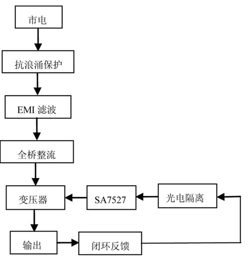


 ,
,  Other ports are the same.
 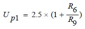 Other cases of the same port.
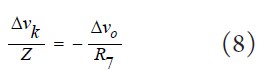


references:
[2]. TL431 datasheet http://
[3]. LM358 datasheet http://
[4]. EL817 datasheet http://
[5]. DB107 datasheet http://
[6]. C13 datasheet http://
[7]. C10 datasheet http://
[8]. R10 datasheet http://
[9]. 18W datasheet http://
8 times
Window._bd_share_config = { "common": { "bdSnsKey": {}, "bdText": "", "bdMini": "2", "bdMiniList": false, "bdPic": "", "bdStyle": " 0", "bdSize": "24" }, "share": {}, "image": { "viewList": ["qzone", "tsina", "tqq", "renren", "weixin"], "viewText": "Share to:", "viewSize": "16" }, "selectShare": { "bdContainerClass": null, "bdSelectMiniList": ["qzone", "tsina", "tqq", "renren" , "weixin"] } }; with (document) 0[(getElementsByTagName('head')[0] || body).appendChild(createElement('script')).src = 'http://bdimg.share. Baidu.com/static/api/js/share.js?v=89860593.js?cdnversion=' + ~(-new Date() / 36e5)];