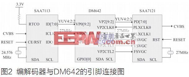
introduction This article refers to the address: http:// However, with the rapid expansion of the video surveillance market, some shortcomings of video surveillance systems on the market are gradually emerging, including high cost, few roads, poor real-time performance and poor picture quality, and users are monitoring due to different monitoring requirements in different occasions. Product flexibility and targeting put forward higher requirements. This design uses TI's TMS320DM642 multimedia processing chip as the main control chip, which keeps the cost within the feasible range, and fully utilizes the high-speed processing capability of the chip core to ensure the real-time performance of the monitoring system. It is a good method to balance the cost and monitoring quality. TMS320DM642 (hereinafter referred to as DM642) is a 32-bit fixed-point DSP chip specially designed for digital media applications. It has a high-performance C64x digital signal processor core and integrates rich peripheral resources such as configurable. Audio and video interface, Ethernet MAC controller, JATG emulator interface, etc. Figure 1 is a block diagram of the entire system. Taking DM642 as the core, it mainly includes video module, storage module, communication module and other peripheral circuit parts. The video module is composed of four encoder chips and one decoder chip. The switching mode is used to support four composite video inputs and one video output display. The storage module extends the off-chip memory SDRAM and FLASH through the EMIF interface of the DM642, and is controlled by the CPLD. FLASH on-chip paging register read and write; communication module part uses CPLD to control parallel port transmission mode, realizes sequential logic and data transmission, so that the whole system accepts the master device control as a slave device to complete a specific image processing operation. System hardware architecture Power management module The DM642 adopts dual power supply mode: CPU core voltage +1.4V, current 793mA; peripheral I/O voltage +3.3V, current 165mA. These two independent voltages need to be strictly in order during power supply, to ensure that the core power supply is powered first, and at the same time should be powered on simultaneously with the I/O power supply to avoid damage to the chip. The power chip uses TI's TPS54310, which uses a 5V power supply on the board to drive two linear regulators, and generates two voltage conversions to generate the required +1.4V and +3.3V. During power-up, ensure that the system clock is in a reset state before the core voltage and I/O supply reach the required voltage to avoid uncontrolled conditions. Therefore, TI's power detection chip TPS3823-33 is used, which can monitor the system's most used +3.3V voltage, and allows each chip in the system to adjust the working state at any time through reset. Clock circuit In order to reduce the off-chip clock frequency and improve system stability, DSP on-chip phase-locked loop (PLL) should be used when designing DSP system. In this design, the external 50MHz clock source is selected, and the PLL is used for 12 times frequency to obtain the 600MHz main frequency required by the CPU. In this design, a 150MHz clock is provided for ECLKIN using a 1/4 CPU clock, and the clock is supplied to the CLK pin of the SDRAM through the ECLKOUT1 pin. The clock frequency used in the whole system is also the 14.31818MHz clock of the video codec chip. It uses the same external crystal oscillator as the DSP main clock. External memory This system is mainly used for video image processing. In the process of processing, massive data will be generated, while DM642 has only 256 KB of RAM. Therefore, it is necessary to expand the large-capacity external memory to meet the needs of data processing. This design uses two Hynx HY57V283220T (4M × 32bit) SDRAM chips to form a 64-bit external RAM space; an AM29LV033C (4M × 8bit) FLASH chip is used to form an external ROM space. The two SDRAM chips are connected in parallel to form a 64-bit bit width and a 32 MB size storage space to a CE0 subspace configured as a synchronous dynamic memory interface and a 64 bit bit width. Video path module In this design, the three video ports VP0VP1VP2 of the DM642 are set to 8-bit BT.656 mode, where VP0 and VP1 are in single channel mode, channel A is used for video acquisition, VP2 is in dual channel mode, and channels A and B are both. Used for video capture. Therefore, up to 4 analog video signals can be acquired simultaneously. In the BT.656 video capture mode, the FIFO space is a total of 2560 KB and is allocated as follows: One 1280 Byte FIFO is dedicated to storing Y sample data; two 640 Byte FIFOs are used to store Cb and Cr data, respectively. Four Philips analog SAA7113 decoder chips are used to convert four analog video inputs. The SAA7113 supports 6 composite video signal CVBS or 1 S-Video input, and the output is 8bit 4:2:2YCbCr format with discrete sync signal or 8-bit BT.656 format digital video signal with embedded sync signal. In the video playback part, the encoder selects one piece of Philips SAA7121, which can convert digital bright signal (YUV) or digital RGB signal into CVBS, S-VIDEO, RGB and other analog signal output, supporting PAL/NTSC system. And support VGA and high definition HDTV output. The pin connection diagram of the codec and DM642 is shown in Figure 2. software design Set the configuration parameters of the DM642 internal module, including VPort video port parameter configuration, SDRAM and FLASH register configuration; I2C bus parameter configuration; codec chip internal register configuration. The system is powered on and initialized. The DM642 simulates the I2C bus timing through the internal software, configures the SAA7113 internal register, and sets its working mode. After that, the DM642 sends the acquisition command to the CPLD. The two parties pass the HOLD and HOLDA handshake signals to realize the bus control handover. At this time, the CPLD is obtained. Bus control, then open the output of SAA7113, write control of the collected video data; when a frame of video data is written into the SDRAM frame buffer, the CPLD turns off the SAA7113 video output, gives up the bus control, and sends an interrupt signal to the DM642. After the DM642 regains control, it uses a specific algorithm for image processing of the captured video data, and buffers the processed video data in SDRAM, and configures the SAA7121 internal register to set its working mode. At this time, the SDRAM is cached. The image data is sent to the SAA7121 for D/A conversion, and the VGA display is sent to the image display through the parallel port; the DM642 re-issues the start acquisition command after the image processing is completed, and the next frame data is collected.
Power Thermistor
Power NTC Thermistor has strong power and strong capability of surge current protection. It has big Material Constant (B value) and small remain resistance as well.
With the properties of fast response, high reliability and long service life, this type of thermistor has a full and wide application range which can be used in conversion power supply, switch power, UPS power, electronic energy saving lamp, electronic ballast, electric heater, CRT and illumination lamp.
Power Thermistor,Material Constant,Temperature Controller,Oven Thermistor Feyvan Electronics Technology Co., Ltd. , http://www.fv-cable-assembly.com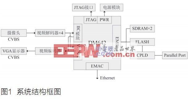
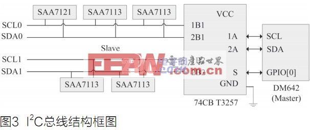
The I2C interface in the DM642 does not support high speed modules, so the I2C bus speed used in this design is up to 400kbit/s. This design uses TI's 4bit 2 select 1 switch SN74CBT3257 to enable the DM642 to receive a set of I2C data at a time. Since the SAA7113 can only be configured with two different device addresses, four SAA7113s cannot be connected simultaneously in one I2C bus. Therefore, the I2C bus must be divided into IIC0 and IIC1. The specific connection method is shown in Figure 3.