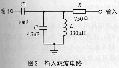
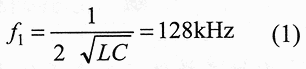
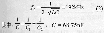
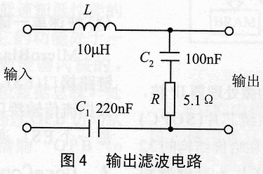
Abstract: Introduce the basic principle of a newly launched power carrier modem chip ST7538, give the main control circuit and interface circuit of ST7538, and discuss some precautions after applying the chip. The power carrier communication using the power line as the communication medium has the advantages of great convenience, maintenance-free, plug-and-play, etc. It is the communication method preferred by people in many cases. ST7538 is another half-duplex, synchronous / asynchronous FSK (frequency modulation) modem chip recently launched by SGSTHOMSON on the basis of power carrier chips ST7536 and ST7537. This chip is designed for power line network communication in the home and industrial fields. Compared with ST7536 and ST7537, it has the following characteristics: * There are 8 working frequency bands, namely: 60kHz, 66kHz, 72kHz, 76kHz, 82.05kHz, 86kHz, 110kHz and 132.5kHz; * Internal integrated power line drive interface, and provide voltage control and current control; * Internal integrated + 5V linear power supply, can provide 100mA current externally; * Programmable communication rate up to 4800bps; * Provides zero-cross detection function; * With watchdog function; * Integrated an on-chip operational amplifier; * It contains a 24-bit programmable control register with checksum; * Adopt TQFP44 package. It can be seen that ST7538 is a powerful, single-chip power line modem. ST7538 is a highly integrated power carrier chip using FSK modulation technology. All functions of sending and receiving data are integrated inside, and can be easily connected with the microprocessor through serial communication. There are automatic voltage control and current automatic control inside, as long as a small number of external devices such as coupling transformers can be connected to the power grid. ST7538 also provides watchdog, zero-crossing detection, operational amplifier, clock output, timeout output, + 5V power supply and + 5V power status output, etc., greatly reducing the number of peripheral devices of the ST7538 application circuit. In addition, the chip complies with European CENELEC (EN50065-1) and US FCC standards. Figure 1 is the internal block diagram of ST7538. 1.1 Sending data When RxTx is low, ST7538 is in the state of sending data. The data to be sent enters ST7538 from the TxD pin. It is sampled at the rising edge of the clock and sent to the FSK modulator for modulation. The modulation frequency is determined by bit0 ~ bit2 of the control register, and the rate is determined by bit3 ~ bit4 of the control register. The modulated signal goes through D / A change, filtering and automatic level control circuit (ALC), and then is transmitted to the power line through the differential amplifier. When the time overflow function is turned on, and the data transmission time exceeds 1s or 3s, TOUT becomes high level, and the transmission state automatically changes to the reception state. This prevents the channel from being used by a certain node (ST7538) for a long time. 1.2 Receive data When RxTx is high, ST7538 is in the state of receiving data. The signal enters ST7538 from the RAI pin of the analog input terminal, passes through a band-pass filter with a bandwidth of ± 10 kHz, and is fed into an amplifier with automatic gain AGC. The filter can be cancelled by setting the control register bit23 to zero. The automatic gain amplifier can automatically adjust according to the signal strength of the power line. To improve the signal-to-noise ratio, the signal passing through the amplifier is fed into a narrow-band filter with the communication frequency as the center and a bandwidth of ± 6kHz. This signal is then demodulated, filtered and phase-locked to become a serial digital signal, and the output is given to the microprocessor connected to ST7538. 1.3 Selection of working mode Through the serial ports RxD, TxD and CLR / T of the microprocessor and ST7538, the data exchange between the microcontroller and ST7538 can be realized. The working mode of ST7538 is determined by the status of REG_DATA and RxTx. The microprocessor's access to the power line can be synchronous or asynchronous. Asynchronous mode only requires RxD, TxD and RxTx, no auxiliary clock signal. When there is no carrier signal, RxD outputs low level. For synchronization mode, CLR / T is required as the reference clock, and ST7538 must be the communication initiator (Master). The access to the ST7538 control register must use the synchronous access method, which requires RxD, TxD, CLR / T and REG_DATA, the rising edge of CLR / T is valid, and the high bit of the transmitted data comes first. 1.4 Reset and watchdog A watchdog is embedded inside ST7538, which can generate an internal and external reset signal to ensure the reliable operation of the CPU. 2 System hardware composition The power carrier communication node module generally includes the following parts: a microprocessor part, a carrier part signal filtering part, and a power line signal coupling and protection part. Figure 2 shows the general power carrier communication module composed of ST7538 and Atmega8L. Here only a brief introduction to the filtering part. The signal filtering part is the key part of the entire module, which includes the input narrowband filter and the output narrowband filter. Figure 3 is the input filter circuit, which uses a parallel current resonance circuit to form a filter circuit to filter out unwanted signals and noise other than the specified frequency. The resonance frequency f1 is Figure 4 shows the output filter circuit, which uses a series voltage resonance circuit to avoid unwanted signal coupling to the power line. The resonance frequency f2 is: The power line coupling part adopts 1: 1 broadband communication transformer, and at the same time, the secondary side adopts the instantaneous voltage suppressor P6KE6V8A to protect the subsequent circuit. 3 Application considerations ST7538 is much more powerful than the early ST7536 and ST7537, and the pin has increased from 28 to 44 pins. It is still very convenient to use, but it also needs to emphasize the following points: ①Pay attention to ensure the power-on reset time and sequence. The reset time of ST7538 is 50ms. When the microprocessor is powered on and reset, there must be enough hardware delay and / or software delay to ensure ST7538 reliable reset. After the ST7538 is reliably reset, it can be initialized. ② ST7538 has 8 communication frequency bands, but only one communication frequency can be used at the same time. To change the communication frequency, you need to adjust the hardware parameters. ③The ST7538 provides only a purely transparent physical layer communication protocol. When the noise signal is mixed into the communication frequency, the ST7538 cannot be distinguished, and it will be demodulated together with the useful signal. Therefore, ST7538 requires users to make their own MAC layer communication protocol to ensure the reliability of communication. ④When the system is composed of ST7538, the communication of multiple nodes can use the bus medium access competitive protocol, such as CSMA (Carrier Sense Multiple Access). However, after all, power carrier communication has a low communication rate and low efficiency. Therefore, you can consider using this zero detection function of ST7538. Using zero-crossing points to achieve synchronous data transmission, and then in a relatively large system can achieve non-bus media competition "TDMA-like" (Time Division Multiple Access) protocol, the protocol is often used in digital wireless communication systems such as GSM. Conclusion ST7538 is a powerful and highly integrated power carrier chip. It is designed for home and industrial environment applications, so it adopts a variety of anti-jamming technologies. Although it uses FSK modulation technology, but does not use spread spectrum technology, there is no advantage of expanding communication, but, because of this, it can achieve reliable communication in a wide noise channel environment. If it can make good use of its multi-band nature, it will be able to overcome the shortcomings of narrowband communication. Dongguan Yijia Optoelectronics Co., Ltd. , https://www.everbestlcdlcm.com
figure 1
1 ST7538 working principle 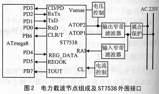
The ST7538 can be placed in a high-sensitivity receiving state by setting bit 22 of the controller.