Audio power amplifiers are widely used in portable devices such as mobile phones, MP3, MP4, etc. In order for the audio power amplifier to work properly, it must contain a bypass voltage control circuit to generate the correct DC bias voltage to make the circuit normal jobs. Here is O. Under the condition of 5μm CMOS process, a bypass voltage control circuit using current feedback to realize hysteresis function is designed. 1 Circuit structure The bypass voltage control circuit includes Schmidt circuit, comparator circuit and control circuit. The overall circuit is shown in Figure 1. The following will be introduced separately. 1.1 Schmidt circuit The widespread application of integrated circuits has added a shutdown function to the chip to reduce the power consumption of the chip. The Schmitt circuit composed of M25 ~ M29 in this design provides this function. When the external pin "SHUTDOWN" voltage Vin is low, M25, M26 are turned on, M27, M28 are turned off, and the D point outputs a high level. At this time, the entire circuit is in the off state, and the internal power consumption is extremely low. As Vin gradually increases, when Vin> VTH (M28), M28 and M29 are both in the conducting state, then the drain voltage of M28 is M28, and the voltage division of M29 to the power supply is approximately VDO / 2. Therefore, M27 is still closed. When Vin continues to rise, the conduction capacity of M25 and M26 decreases, which causes the source voltage of M27 to drop. When VGS (M27)> VTH (M27), M27 starts to conduct, causing the voltage at point D to drop sharply, further causing M25, M26 The continuity of is weakened until the end. At this time, the output is turned over, and the D point outputs a low level, and the circuit turns to normal operation. The characteristic of the Schmitt trigger is that it can convert a slowly changing voltage signal into a rectangular pulse with a steep edge, so even if the voltage of the external pin "SHUTDOWN" changes slowly or contains noise, the circuit can work normally; at the same time It can be seen that the circuit will work normally only when the input is greater than a certain voltage. This design improves the anti-interference ability of the circuit. 1. 2 voltage comparator circuit The comparator is used to compare two input analog signals and thus produce a binary output. Normally, the comparator works in a noisy environment and detects changes in the signal at the threshold. When a signal containing noise is added to the input of a comparator without hysteresis, the output of the comparator will be full of noise, and even oscillation may occur. Therefore, the design often uses positive feedback to achieve the hysteresis function, so that the circuit has a certain ability to resist noise. This kind of positive feedback is often divided into external positive feedback and internal positive feedback, and because the high-precision resistance required for external positive feedback is difficult to achieve in integrated circuits, internal positive feedback has been more widely used. In this design, the main function of the voltage comparator is to compare the size of the bypass voltage and the reference voltage, and output a signal to the control circuit to determine whether to charge the bypass capacitor. Its circuit structure diagram is shown as in Fig. 2. When PD is low. The comparator works normally. When the voltage at the “+†terminal is lower than the voltage at the “-†terminal, the leakage current of M1 is greater than the leakage current of M2. The excess current charges the capacitor Cj (equivalent parasitic capacitance from this point to ground), and the gate voltage of M6 rises. High, when | VGS6 | <| VTP |, M6 is cut off and the comparator outputs low level; in the same way, when the voltage at the “+†terminal is higher than the voltage at the “-†terminal, the capacitor Cj (the equivalent of this point to ground) Parasitic capacitance) discharge. The gate voltage of M6 decreases, M6 is saturated and turned on, and the comparator outputs a high level. M8 ~ M12 are the current feedback part. When the comparator outputs a high level, the switch tubes M9 and M12 are turned on, M11 and M8 form a current mirror structure, when M11 and M8 are in the saturation region, the current mirror works normally and M11, mirror M8 leakage current and feedback back to A Point to change the threshold voltage VTRP- of the negative transition of the comparator to achieve the purpose of hysteresis. Then by adjusting the width-to-length ratio of M11 and M8 tubes, the size of the current fed back to point A can be changed, thereby changing the negative turning threshold voltage of the circuit. At this time, the positive turning point and the negative turning point of the comparator are different. The comparator circuit has a bistable characteristic, and its width is: This width voltage indicates the maximum noise amplitude allowed by the comparator. Compared with the circuit described in the literature that uses internal voltage positive feedback to achieve hysteresis, the current feedback method avoids the use of positive and negative feedback at the same time, making the circuit performance more stable; on the other hand, it also reduces MOS The number of times the tube status changes reduces the comparator transmission delay. When PD is high, M13 is turned off, M14 is turned on, so that M5, M7, and M10 are in the off state, and the entire circuit is in a low power consumption state. 1.3 Control circuit The function realized by the control circuit is to generate the reference voltage required by the comparator and charge and discharge the bypass capacitor. In Figure 1, the gate voltages of M17 and M18 are generated by the bias circuit of the amplifier. When PD is low level, the switch M15 is turned on, adjust the value of R1, R2, make the voltage at point B equal to VDD / 2, and use the voltage at point B as the forward turning voltage of the comparator, at this time switch M19 Turn on. The circuit charges the bypass capacitor CB and uses the voltage at point C as the positive input of the comparator. When the voltage on the capacitor is lower, the comparator outputs a low level and M21 is turned off; when the voltage on the capacitor is higher than the forward corner voltage, the comparator outputs a high level and M19 is turned off, the circuit stops charging the bypass capacitor, At the same time M21 is turned on. The voltage at point C at this time is: Where: VC + is the voltage on the capacitor after M21 is turned on; VC- is the voltage on the capacitor before M21 is turned on; τ is the time constant, τ = (RB + R) C; RB is the equivalent of point B to ground resistance. It can be seen that after a period of time, the voltage on the bypass capacitor will be approximately equal to the voltage at point B, that is, VDD / 2, then the required bypass voltage is obtained. At the same time, considering that the "POP" noise of the audio power amplifier when it is powered on or powered off is caused by the instantaneous jump of the bypass voltage, the bypass capacitor can be appropriately increased to increase the rise and fall speed of the bypass voltage. Play the role of reducing "POP" noise. When PD is high. M16 is off, the circuit does not work. Wu Hui Zhang Tao Modern Electronic Technology 2 Simulation results The design uses Candence Spectre simulation tools for simulation, the process used is China Resources Shanghua O. Typical model of 5μm N-well CMOS process. Figure 3 shows the output curve of the bypass voltage in this design. The "SHUTDOWN" pin is active low, and the output curve will show a small spike when the circuit changes from the off state to the working state. This is because the voltage on the bypass capacitor is slightly higher than node C, and the capacitor will have a small Discharge process. At normal temperature, the output begins to stabilize at 2.5 V at about 3.4 μs. When t = 7.5μs, the output is 2.501 6 V, and the error is O. 064%. The static power consumption of the circuit is O. 685 mW. Figure 4 shows the positive voltage of the voltage comparator from 2.0 to 3. OV changes and from 3. O ~ 2. 0 V changes, the output curve of the comparator. It can be seen that the comparator has a positive threshold voltage and a negative threshold voltage. The inequality between the two indicates that the ability to suppress noise by introducing a hysteresis circuit is significantly enhanced. Figures 5 and 6 show the positive and negative transmission delays of the comparator, respectively. It can be seen from the figure that the comparator's positive transmission delay is 7.632 ns, and the negative transmission delay is 35.32 ns. For most chips, this order of magnitude of delay is negligible. 3 Conclusion It can be seen from the above simulation results that the bypass voltage control circuit of this design can produce a stable output bypass voltage and has a certain noise suppression capability. In addition, the static power consumption of the entire circuit is low, and the signal delay time is short, which can be widely used in various audio amplifier circuits.
Wire Packaging Spool, Magnet Wire Reel, Magnet Wire Spool, Packing Wire Spool NINGBO BEILUN TIAOYUE MACHINE CO., LTD. , https://www.spool-manufacturer.com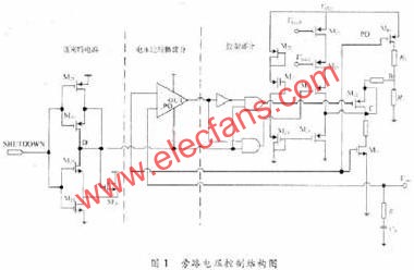


2)High speed custom labeling and printing on flanges available – even on short runs
3)One piece molded construction for strength and precision
4)Appealing designs as well as ergonomics (no sharp edges)
Type
Weight
(gram)
d1
(mm)
D1
(mm)
d2
(mm)
D2
(mm)
H1
(mm)
H2
(mm)
d3
(mm)
A1
(mm)
A2
(mm)
d4
(mm)
E
(mm)
PC-70
40
70
38
70
85
20
7
7
PC-80
70
80
50
64
80
20
8
8
7
20
PC-83
70
83
45
100
120
20
10
10
PC-100A
110
100
45
70
88
20
9
9
PC-100B
100
100
45
100
120
20
10
10
PC-125A
180
125
65
100
120
20
10
10
7
20
PC-125B
170
125
70
100
120
20
10
10
PC-130A
200
130
65
100
120
22/25
10
10
PC-130B
210
130
65
100
120
22
10
10
SH-16
230
150
90
100
124
30
12
12
12
26
PC-185A
400
185
128
155
178
30
11
11
PC-185B
500
185
128
155
178
30
11
11
PC-185C
500
185
130
160
180
30
10
10
PC-220A
660
220
110
155
185
40
15
15
12
42
PC-220B
660
220
110
155
185
38
15
15
15
38
PC-220C
660
220
110
155
185
30
15
15
14
38
PC-250
870
250
110
155
185
40
15
15
12
42
PC-300A
1400
300
180
170
200
32
15
15
17
45
PC-300B
1400
300
180
170
200
100
15
15
20
125
PC-355
1950
355
224
160
200
36
20
20
26
50~80
PC-410
4550
410
310
180
228
70
24
24
PC-500A
8450
500
315
180
250
40
35
35
26
70~100
PC-500A1
8450
497
315
180
250
40
35
35
26
70~100
PC-500B
8600
500
250
250
300
56
25
25
26
70~100
PC-500B2
9020
500
250
240
290
40
25
25
26
70~100
PC-500C
8600
500
250
235
300
56
20
20
26
70~100

Significant product benefits:
1)A full line of spools in a variety of standard sizes