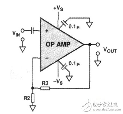
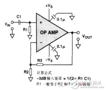
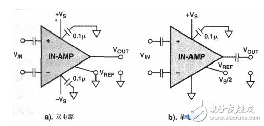
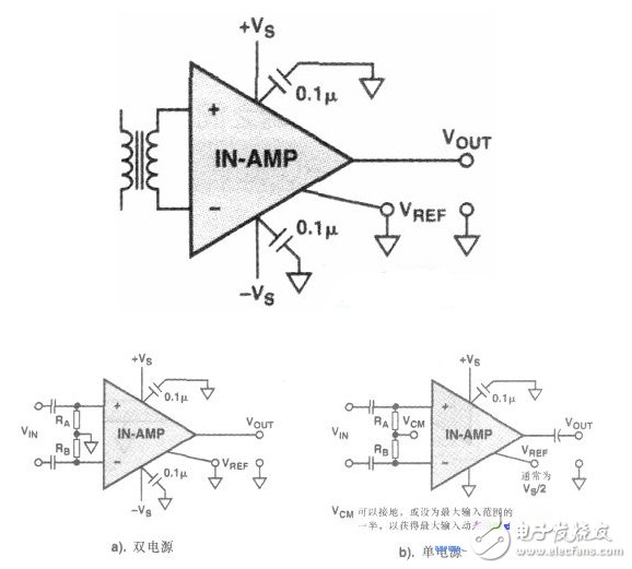
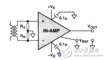
One of the most common application problems is the absence of a DC loop that provides a bias current in an AC-coupled op amp or instrumentation amplifier circuit. As shown in the figure above, a capacitor is connected in series with the non-inverting input of the op amp to achieve a simple method of isolating the DC component of the input voltage Vin, which is especially useful in high gain applications, even in those applications. A small DC voltage at the input of the amplifier limits the dynamic range and even causes the output to saturate. However, adding a capacitive coupling to the high impedance input without providing a DC path for the current at the non-inverting input can cause problems. Missing DC bias current loop when AC coupling In effect, the input bias current flows into the coupled capacitor and charges it until it exceeds the nominal value of the common-mode voltage of the amplifier input circuit or causes the output to reach its limit. Depending on the polarity of the input bias current, the capacitor will charge to the positive or negative voltage of the supply, and the closed-loop DC gain of the amplifier amplifies the bias voltage. This process can take a long time. For example, a FET input amplifier, when the bias current of lpA is coupled with a 0.1-milli capacitor, its charging speed is 10/12 /10 of I/C. -7 power = lO éœ / s. If the gain is 100, the output drift is 0.06V per minute. Therefore, the general laboratory test (using an AC-coupled oscilloscope) can not detect this problem, and the circuit will not be used until a few hours later. problem appear. Obviously, it is very important to avoid this problem altogether. The figure above shows the solution to this problem. Here, a resistor is connected between the input of the op amp and ground to provide a ground loop for the input bias current. The offset voltage is generated for the input bias current. Minimal, when using a bipolar op amp, the bias currents of the two inputs should be equal, so the resistance of Rl should normally be set equal to the parallel resistance of R2 and R3. However, it should be noted that this resistor R1 always introduces some noise into the circuit, so a compromise is made between the input impedance of the circuit, the size of the input coupling capacitor, etc., and the typical resistance value is between 100000 Ω and 1 MΩ. A similar problem can also occur in the instrumentation amplifier circuit. The figure above shows an instrumentation amplifier circuit that uses two capacitors for AC coupling. There is no return path for the input bias current. This problem is achieved with dual and single supply. Common in instrumentation amplifier circuits. This type of problem can also occur in transformer-coupled amplifier circuits. As shown in the figure below, this problem can occur if a DC-to-ground loop is not provided in the transformer's secondary circuit. The above figure and the following figure are simple solutions for these circuits. Here, a high-resistance resistor (RA, RB) is connected between each input and ground, which is a simple circuit suitable for dual-supply instrumentation amplifier circuits. And a practical method. These two resistors provide a discharge loop for the input bias current. In the dual power supply example shown in Figure 5, the reference terminals of both inputs are grounded. In the single-supply example shown in Figure 5, the reference terminals of the two inputs are grounded or connected to a bias voltage, typically with a bias voltage of l/2 of the maximum input voltage. The same principle can be applied to the transformer coupled input circuit (above), unless the secondary pole of the transformer has a center tap, it can be grounded or connected to VCM. In this circuit, due to the mismatch between the two input resistors and both ends A mismatch in the input bias current produces a small offset voltage error. In order to minimize the offset error, a resistor can be connected between the two inputs of the instrumentation amplifier (that is, bridged between the two resistors), and its resistance is about 1/10 of the first two resistors. Provides a reference voltage for the amplifier and ADC
As LCD display in YFJ company that we usually use it to military grade battery ,especially Lithium-ion batteries ,for these battery applications ,we have obvious advantage is that we focus more on shor circuit protection which we follow the US military standard.
Short circuit protection:The following test shall be performed. Charge batteriesas specified in ; use of 4.6.3 is permitted. Measure and record the OCV. Short each battery across all the positive and negative terminals with a total external resistance not greater than 50 milliohms. After one hour remove the short from across the terminals. Measure and record the OCV. Stabilize batteries at the normal conditions of 4.3.1 for not less than 2 hours. Chargebatteries in accordance with 4.6; use of 4.6.3 is permitted. Stabilize batteries at normal conditions for not less than 2 hours, then discharge the battery in accordance with 4.7.2.3. The battery shall meet the requirements of 3.7.2.3.
Li-Ion Battery With Lcd Display
Charge voltage: 16.8V
Nominal voltage : 14.8V
(4S7P)
Initial impedance : 120mΩ
Nominal capacity: 19.6Ah
Minimum capacity: 19.4Ah
Communication methods : SMBUS data communication
Electricity quantity show: LCD Electricity quantity show
Charge current: Standard Charging::0.2C5A (3.9A)
Rapid charge: 0.5C5A C(9.8A) Max
Standard Charging method : 3.9A(0.2C5A) CC(constant current)charge
to 16.8V,then CV(constant voltage 16.8V)charge till charge current decline to
≤196mA(≈0.01C5A)
Charging
time:Standard Charging: 6.5hours(Ref.)
Rapid charge: 3.5 hours(Ref.)
Max.discharge current: 9.8A(0.5C5A)
Discharge cut-off voltage: 10.0V
Cycle life (0.2C5A/0.2C5A) : 500 items,≧80%DOD;
300 times,≧80%DOD
Operating
temperature : Charging: 0℃~45℃
Discharging:-20℃~+60℃
Li-ion Battery With LCD Display Li-Ion Battery With Lcd Display,Battery Charger With Lcd Display,Battery Pack With Lcd Display,Rechargeable Battery Pack With Lcd Display YFJ TECHNOLOGY (HK) CO.,LIMITED , http://www.yfjpower.com