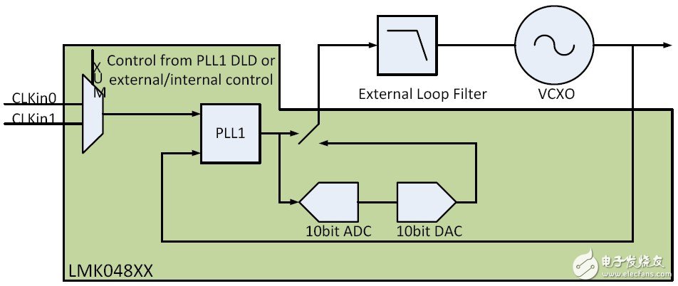
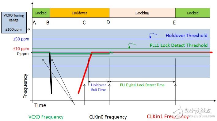
Summary This article first introduces the holdover functions and metrics of TI's next-generation clock product, the LMK0480X, and its application in a new generation of wireless C-RAN networks. Through the analysis of the LMK0480X holdover, it is proved that the LMK04808 fully meets the clock switching requirements of the communication network. 1, the introduction of the Holdover function In the current communication system, whether it is wired or wireless, it is a clock synchronization system. The reference clock is transmitted from the sink source to each device in the system through the network; in order to improve the stability of each device in the system, and in order to improve the flexibility of the device in the system for different applications, generally more than one reference clock is input to the device. in. When the clock unit in the device switches between the reference clocks of these inputs, the clock unit's output should maintain performance and clock stability. This requires the clock circuit to have a holdover function and support reference clock hitless switching. The so-called holdover function in the analog clock circuit of the past is that when the clock switching occurs, the charge pump of the phase detector is forced to output to VCC/2; however, in some cases, the difference between the charge pump voltage and the VCC/2 when the clock is locked Larger, so in the process of clock switching, the output clock may jump beyond the allowable range of the system, causing the system's timing disorder. In TI's latest clock debounce chip LMK048XX series, a charge pump voltage tracking circuit has been added; this circuit samples the charge current voltage in real time and saves it to the integrated DAC of the chip; when the chip is in the process of input clock switching, the charge pump voltage The output is switched to the output of the DAC so that the voltage-controlled voltage changes very little before and after the reference clock is switched, ensuring the stability of the system clock. The Holdover function of the LMK0480XX family of clock devices is a true hitless switch. The following sections detail the entire process of holdover and related metrics. 2, LMK0480x series product holdover function introduction The LMK048xx series is TI's next-generation clock debounce chip, which uses a two-stage phase-locked loop cascade architecture. The first-stage phase-locked loop uses a narrow-band loop filter and an external VCXO to perform debounce on the input reference clock. The second-stage loop filter mainly utilizes a high-performance internal phase-locked loop to generate various clocks required by the system. The Holdover feature mentioned above is a feature of the first-stage phase-locked loop. Figure 1 LMK0480X holdover architecture The figure above is a functional block diagram of the LMK048XX holdover. Among them, CLKin0 and CLKin1 are two reference clocks from the network respectively, and one is selected as the clock chip and the main clock of the system. When the master/slave switchover or service switchover occurs on the network device, the reference clock of the clock chip also switches. The conditions for triggering the reference clock switch can be a. DLD status of PLL1, b. Hardware control of external pins, c. Internal register control. In the following discussion we assume that the switch is triggered by the DLD state of PLL1. When the LMK048XX holdover function is enabled, a complete reference switching process is shown in the following figure. It is mainly divided into the following steps: Figure 2 LMK0480X holdover process Step1: PLL1 is normally locked at CLKin0, PLL1 DLD is high; LMK048XX integrated counter ADC tracks the voltage control voltage of VCXO and updates the integrated counter DAC, the update rate is PDF/DAC_CLK_DIV, rising or falling one LSB in each update cycle. Step2: When CLKin0 is lost for some reason or a large frequency error occurs, the phase error of PLL1 exceeds the lock window (PLL1_WND_SIZE), DLD is low; when DLD is low, the ADC stops tracking the voltage control voltage and updates the DAC, DAC The output maintains the voltage-controlled voltage at the last lock; DLD pulls low while triggering the LMK048XX to enter the holdover state, and the internal switch switches the VCXO's voltage-controlled voltage to the DAC output.
- Wall Socket Expansion allowing you to expand one in wall socket to multi outlets, as well as to add more functions, e.g. socket plus USB ports, or with surge protector, or with overload protection.
- Multiple
Outlets allowing you to plug in multiple electrical devices.
- Compact Wall Expansion is also convenience as travel power adapter from its weight and size point of view.
- PC/ABS flame
retardant, phosphor bronze+pure copper.
- Space saving and cost saving
- We have been doing OEM service for Germany
customer since the very beginning time when
we started power strip manufacturing.
Now we still continue with OEM/ODM services and
doing our own design as well.
- Own factory
Wall Socket Expansion Wall Socket Expansion, Compact Wall Expansion, USB Wall Socket, Multi Outlets Wall Socket ZhongShan JITONGLONG Plastic Hardware Co. Ltd. , https://www.toukoo-electronics.com