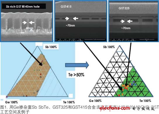
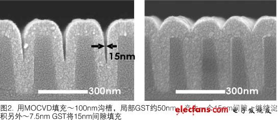
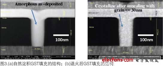
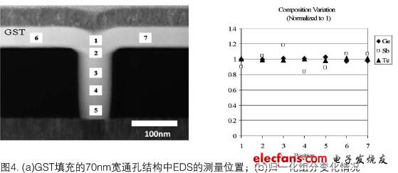
In order to achieve the next milestone in the PCM's improved high-performance/high-density development process, one approach being taken is to constrain the PCM material (ie GST) with a conformal deposition process in a high aspect ratio device cell with a cross-section size of 10-100 nm. . By simultaneously addressing multiple cells and eliminating cell-to-cell interference with improved thermal isolation and allowing high density integration, high constraints can reduce the reset current to increase the write bandwidth. Smaller constraining units also increase device speed. A chemical vapor deposition (CVD) based process can fill the aspect ratio 3:1, section 7.5 & TImes; 60 nm dash structures, achieving a reset current of 160 μA and a settling speed of 50 ns. The atomic layer deposition (ALD) based process can fill the aspect ratio 3:1, section 7.5 & TImes; 14nm dash structures, achieving a reset current of 90μA and a settling speed of 30ns. Compared with the planar structure, the deposition thickness in the constrained cell structure is also greatly reduced, which increases the deposition yield. In order to obtain a suitable threshold voltage, the planar device structure requires at least 30 nm of thickness GST to be deposited; and the constraining cell requires only half of the cell size in the contact region, for example 3.75 nm for a 7.5 nm thick structure, so that the deposition time is also less than ten. About one point. The successful use of CVD or ALD deposited GST alloys for PCM requires very reliable conformal deposition in constrained structures with suitable material properties of 10-100 nm high aspect ratio, including voidless deposition, The adhesion of SiO2 and the upper/lower metal electrode is good, and the material properties are stable at 400 ° C, and can withstand subsequent device processing steps. Alloys are also needed that have low reset currents, high cycle life of at least 1&TImes; 106, 10 years data hold temperature above 85 °C, short set time or fast set, low impedance in set or crystalline state High impedance when reset or amorphous. Meeting these requirements will provide a wide range of resistivity between the amorphous phase and the crystalline phase, which is desirable for multi-level cell storage (MLC) applications. ATMI has developed an MOCVD process (metal organic chemical vapor deposition) capable of filling structures with an aspect ratio greater than 3:1 and a size less than 15 nm, see Figure 2. The CVD process is the preferred process because it produces faster batches than the ALD process and has the same size batch. The ATMI MOCVD process is very efficient because it is designed to use metal organic precursors that can be processed at lower temperatures than typical CVD processes. ATMI also acquires the material physical properties and excellent electrical properties required for basic and advanced device applications, including the feasibility of DRAMs with a settling speed of 12 ns. This paper describes the electrical properties obtained from the development of mature MOCVD deposited GST material properties. One is the 325GST alloy deposited by MOCVD, which reduces the reset current by 2-3x compared to the PVD GST alloy, indicating the possibility of NOR flash memory applications. The second is the 415GST alloy deposited by MOCVD. Its set speed is 65ns, the 10-year data temperature is 118°C, which is nearly 20°C higher than that of PVD GST 225 alloy. It is expected to have higher speed and higher temperature in SCM. Application under the environment. GST fill with high aspect ratio structure In the study done, the high aspect ratio structure can be properly filled with GST of many different components. Figure 1 shows the various component tests performed. GST conformal deposition (the orange region at the lower left of the GST phase diagram) was obtained, including a structure that successfully filled a 40 nm high aspect ratio hole and a Ge-doped Sb-rich SbTe aspect ratio of 5:1. The green area at the lower right of the GST phase diagram is a Te-rich GST alloy with a Te content greater than 50%, including the recently obtained 325 and 415 alloy components. High-performance PCM applications generally require high Te% GST alloys because of their low crystallization temperatures. Since the general deposited film is crystalline, it is not flat or conformal, which is a result of the high deposition temperature required for typical precursors in the deposition. Figure 1 shows the filling of GST325 and 415 in high aspect ratio vias using the ATMI MOCVD process. In our recent 300mm MOCVD process demonstration, it was also successful to fill a 15 nm small trench structure with a smooth and conformal film, with a Te composition of ~50% (Figure 2). The GST naturally deposited in the constrained structure may be completely amorphous and can be converted to a crystal after annealing, as shown in Figures 3a and 3b, respectively. Note that very fine grains of ~5 nm were obtained. The very small grain size is important for future GST shrinking to less than 10 nm. In the work done, the components in the GST-filled holes are very consistent. Figures 4(a) and 4(b) show the normalized composition measured by EDS. The distribution of Ge, Sb and Te in positions 1 to 5 (corresponding to the top to bottom of the via structure) in the via hole is very uniform. The composition of positions 6 and 7 (corresponding to the outer two sides of the via) is also similar to that of positions 1-5, indicating that an excellent composition distribution is obtained during film conformal deposition. The measured Sb distribution varies greatly, probably due to the inaccuracy of measuring Sb with EDS, because the signal is small and the accuracy is low. Device performance 2Pans Buffet Server,Buffet Server Warming Plate,Buffet Server Warmer,2Pans Buffet Server Warmer Shaoxing Haoda Electrical Appliance Co.,Ltd , https://www.zjhaoda.com