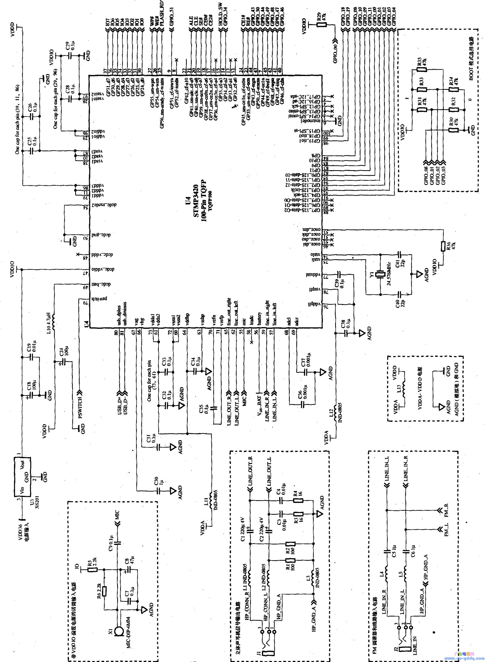
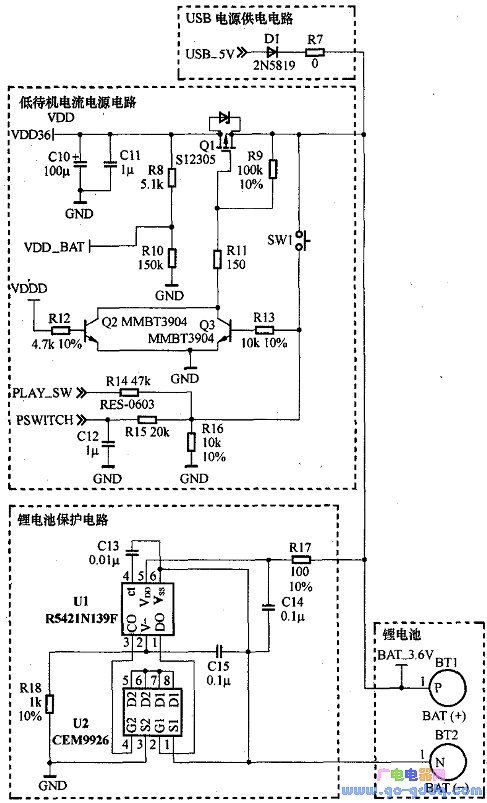
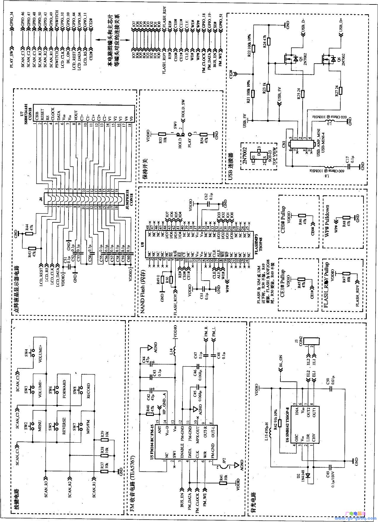
Currently, the MP3 main chip with a significant market share includes not only the Actions ATJ series introduced earlier but also the STMP34xx and STMP35xx series from American Sigmatel. In recent years, the STMP3410 has been widely adopted by MP3 manufacturers due to its cost-effectiveness, integration, functionality, and compatibility. It once held over 80% of the market share, making it a popular choice among users. Although its usage has slightly declined recently, the large number of existing devices still requires maintenance and support. This article will explore the application circuit for the STMP3410/S17MP3420 main chips. The STMP3410 and STMP3420 support USB data transfer, decoding of MP3/WMA formats, and other music formats through firmware updates. They also include features like WMA copyright management, LED/LCD display drivers, FM radio control, and volume adjustment. The chip integrates a high-efficiency DC-DC converter, allowing various power supply configurations, such as using a single AA battery for over 35 hours of continuous operation. The STMP3420 is an upgraded version of the STMP3410, offering support for MP3 encoding and direct playback from external sources, while maintaining similar basic functions. The STMP3410 comes in three package types: 100-pin TQFP, 144-pin TQFP, and 1.44-pin (fp) BGA. The STMP3420 is available in 100-pin TQFP and 144-pin fpBGA packages. Pin assignments are shown in Figure 1. Figure 1 This article uses the Feige FKDS00 MP3 player as an example to explain the main components of the circuit. The circuit diagram is based on the public version of the Sigmatel STMP3420 program. Other circuits using the STMP3410/STMP3420 solution are generally similar and can be used as a reference. 1. Main Chip Figure 2 Figure 2 shows the application circuit for the STMP3420 (U4) in a 100-pin TQFP package. Each pin's name is labeled inside the chip box. Note that the pin names and circuit terminal names differ. For example, the chip’s 37th pin is named GP31_d7, while the corresponding terminal is 107. Be careful when interpreting the diagram to avoid confusion. The main chip's external memory data bus ports (GP24_d0 to GP31_d7, pins 30 to 37) are connected to the flash memory U8's I/O1 to I/O7 for data transmission. The main chip has multiple GPIOs used for controlling peripheral circuits like buttons, displays, and radio functions. The 75th and 74th pins (XTALI and XTALO) connect to an external crystal oscillator Y1 and capacitors C40 and C41, forming a 24.576 MHz oscillator. The 81st and 80th pins (USBD- and USBD+) handle USB data transfer. The circuit includes two grounding types: GND (general or digital ground) and AGND (analog ground). Separating them prevents interference between digital and analog circuits. These grounds should be placed separately on the PCB, typically connected at the bottom of the main chip. It's important to note that the peripheral capacitors of the main chip have labels like "one cap per pin," meaning each pin has a separate capacitor. For example, "one cap per pin (73, 61)" indicates that capacitors C32 and C33 are connected to pins 73 and 61 of the STMP3420 and AGND, respectively. 2. Power Circuit Figure 3 The STMP3420 contains a power management unit with two DC-DC converters. It supports single or dual batteries (alkaline or NiMH), lithium batteries, or external DC power. The power supply mode is controlled via DCDC_MODE0, DCDC_MODEL, and DCDC_MODE2. The table below shows the different configurations. Note that DCDC_MODE0 and DCDC_MODEL are only applicable to the 144-pin package. For the 100-pin package, only DCDC_MODE2 (pin 54) is used, allowing two power modes: one using a single alkaline battery or Ni-MH battery (DCDC_MODE2 = 1) and another using a lithium battery (DCDC_MODE2 = 0). In this case, the circuit uses a lithium battery, so DCDC_MODE2 is grounded, and only the #1 DC-DC converter operates in buck mode, providing 1.8V output. Figure 4 Figure 4 illustrates the power supply circuit outside the main chip, including the USB power supply, low standby current power supply, lithium battery protection, and the lithium battery itself. The USB-5V voltage is applied to the low standby current power supply and the lithium battery through diode D1 and resistor R7 (0Ω). When the power button (play/pause) is pressed, Q3 turns on, enabling Q1 to provide 3.6V to VDD36, which powers the 3-terminal regulator U3. The output voltage VDDIO supplies the external circuit, and the main chip receives the processed voltage for internal use. This low standby current design significantly reduces power consumption and extends battery life. The integrated circuits U1 and U2 form a lithium battery protection circuit. U1 (R5421N139F) protects against overcharging (4.0V–4.4V) and over-discharging (2.0V–3.0V). U2 (CEM9926) is a power device with two N-channel MOSFETs, acting as switches controlled by U1. 3. Flash Circuit Figure 5 The flash circuit is located at the bottom of Figure 5. Flash memory (NVM) is commonly used in storage devices like MP3 players. NAND flash memory offers fast read/write speeds, hardware protection, and convenient interface. The flash memory in the figure is U8, which may be Samsung K9F1G08U0M (128MB), K9F2GO8U0M (256MB), etc. Its working voltage is 2.7V–3.6V, with 100k erase cycles and 10-year data retention. The I/O0–I/O7 of U8 are connected to the main chip’s d0–d7 (pins 30–37), enabling mutual data transfer. The small dashed blocks in Figure 5 represent pull-up or pull-down resistors for signal control. Other flash memory options include HY27UF082G2M (128MB) and TC58NVGOS3AFT (128MB) from HY and Toshiba. 4. LCD Circuit The LCD circuit is shown in the upper dotted line of Figure 5. It consists of the Samsung S6B0724A01 module, a 65×132 dot matrix display capable of showing characters and graphics. It interfaces directly with the main chip via standard data buses, control lines, and power lines. The module operates at 2.4V–3.6V, with a drive voltage of 4.5V–15.0V and a quiescent current of less than 10μA. The module connects to the main chip through connector J4, where LCD_RST, LCD_RS, LCD_CLK, and LCD_DATA are connected to the STMP3420’s GP1044, 11, 10, and 4 ports for control and data transmission. 5. Backlight Circuit The backlight circuit is at the bottom left of Figure 5, composed of SM8142. It works with inductor L15, diode D2, and capacitor C49 to generate a 120V pulse voltage. The backlight is controlled by the BL-ON terminal (GPIO_09), with brightness adjusted via resistor R42. A higher resistance increases brightness. The backlight is turned off when the ENA terminal (pin 5) is low. 6. Button Switch Circuit The button switch circuit is shown in the top-left dotted line of Figure 5. The STMP3420 uses GPIO_43, 46, 47, 48, 49, 50 for scanning keys. The circuit includes three scan inputs (SCAN-R1/R2/R3) and three outputs (SCAN-C1/C2/C3), with seven pushbuttons connected for user interaction. 7. USB Connection Circuit The USB connection circuit is shown in the bottom-right dotted line of Figure 5. The MINI USB socket CN1 provides +5V, USB_D-, USB_D+, and ground through L9. USB_D- and USB_D+ are connected to the STMP3420’s 81st and 80th pins via resistors and FETs for data transmission. 8. FM Radio Circuit The FM radio circuit is in the left-middle dotted line of Figure 5. It includes the FM module U5 (FM104BE), which contains the TEA5767 IC. The FM module is controlled by signals from the main chip’s 3rd, 4th, 5th, and 6th pins. Stereo audio signals from U5’s 8th and 9th pins pass through capacitors and are added to the STMP3420’s LINE-IN-R and LINE-IN-L terminals for amplification and output. 9. FM Tuner / Line Input Circuit The FM tuner and line input circuit is at the bottom-left of Figure 2. It allows external audio input from jack J2. Left and right channel signals are applied to the STMP3420’s 59th and 57th pins via inductors and capacitors. The main chip processes the signal for MP3 encoding, recording, and output. The FM radio output is also routed to the same terminals for playback. professional power amplifier,high powered amplifier,digital amplifier,class d power amplifier Guangzhou Aiwo Audio Technology Co., LTD , https://www.aiwoaudio.com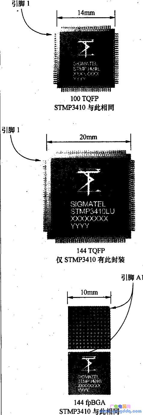
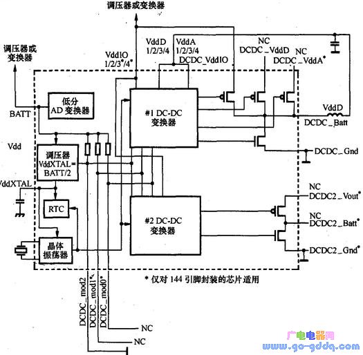
DCDC_MODE2:0
Type of power supply used
#1 DC-DC converter
#2 DC-DC converter
111*
One alkaline or nickel metal hydride battery (0.9V ~ 1.5V)
2-channel boost mode (1.8/3.3V)
Shut down
110*
Reserved
Reserved
Reserved
10l★
One alkaline or nickel metal hydride battery (0.9V ~ 1.5V)
3-channel boost mode (1.8/1.8/3.3V)
Shut down
100★
Reserved
Reserved
Reserved
011
Lithium battery (3.0V ~ 3.6V)
One channel buck mode (1.8V)
Shut down
010★
External power supply
Shut down
Shut down
001★
Two alkaline or nickel metal hydride batteries (1.8V to 3.0V)
One channel buck mode (1.8V)
One channel buck mode (3.3V)
000★
Lithium rechargeable battery (3.3V to 3.6V)
One channel buck mode (1.8V)
One channel buck mode (3.3V)
Class AB Amplifiers
Class D Amplifiers
A power amplifier (PA) is a critical audio component designed to take weak audio signals from pre-amplifiers, mixers, or source devices and boost them to levels capable of driving speakers, delivering loud, clear, and dynamic sound. As the final stage in an audio chain, power amplifiers are essential in everything from home stereos to massive concert systems, balancing raw power with precision to ensure audio integrity.
Â
Â
Applications Across Industries
1. Home Audio
ï‚·Use Cases: Powering bookshelf speakers, floor-standing speakers, or subwoofers in 2.1/5.1 systems.
ï‚·Example: A 2-channel Class AB amp (100W x2) paired with a CD player and stereo speakers for music playback.
2. Professional Audio
ï‚·Live Events:
ï‚·Large-scale concerts use multi-channel Class D amps (e.g., 4x1000W) to drive line array speakers.
ï‚·Features like bridge mode (combining channels for mono subwoofer power) are critical.
ï‚·Installed Systems:
ï‚·Commercial spaces (hotels, schools) use 70V line amps for distributed audio, ensuring consistent volume across zones.
3. Automotive Audio
ï‚·High-Power Setups: Class D amps (e.g., 2000W mono for subwoofers) deliver deep bass from car batteries (12V systems).
ï‚·Space-Saving Design: Compact Class D modules fit under seats or in trunks without excessive heat.
4. Studio Monitoring
ï‚·Precision Amplification: Class AB amps with low THD (<0.01%) ensure accurate sound for mixing and mastering.
Nearfield Monitors: Dedicated amps for small speakers placed close to the listener in recording studios.Â
A power amplifier is the backbone of any audio system, translating electrical signals into the sound that entertains, informs, and moves audiences. Whether delivering subtle nuances in a jazz recording or the thunderous bass of a rock concert, its ability to balance power, efficiency, and precision makes it indispensable in the world of audio engineering.Â