Oil filters have been popular among enthusiast and professionals
alike for its great value and great contributions in boosting engine power. Due
to the demands of application tested technology for performance enhancements,
Oil Filter upgrades or performance oil filters have been included in most
popular vehicle specifications to achieve the best possible fuel economy ever
developed for all engine types. By letting your engine consume fuel at its
finest form, wastage is minimized and overall output is substantially
increased. Keeping the part in good working condition is necessary to ensure smooth
operations while maintaining engine precision that enabling you to continually
rake performance and fuel efficiency gains. Because the your fuel reservoir may
have debris and rust particles, your engine oil filter works in isolating the
debris and other contaminants so it would not reach your engine systems and
clog engine channels which often results to leakage and more serous engine
problems. Newer versions of this engine component feature thicker canister
walls to establish strength offering long lasting and reliably efficient
service. Ideal for ever demanding high performance driving applications, their
high grade and extremely durable construction sustains smooth operations over
extreme pressure and heat minimizing the risks of failure. Investing with
quality and heavy duty oil filter makes a great valued investment that
unleashes your vehicle full potential to achieve the best possible fuel economy
your vehicle could deliver. By keeping the gains of precision flow of cleaner
oil at faster rate due to consistent pressure, reaching peak combustion
efficiency is conveniently possible. Thanks to the continuously increasing fuel
rates, the need to consider fuel economy has been emphasized. Our site covers
your general automotive needs as we carry a wider selection for heavy duty
stock or performance oil filter replacements available for specific vehicle
applications. Go on and seal your oil filter deals with us to order your needs
right at your fingertips
Car manufacturers often suggest changing
oil filters every other time you have your oil changed. Most parts and oil
manufacturers, however, say to replace oil filters with every oil change, which
should occur every 3,000
miles or three months (whichever comes first).
Oil Filter Oil Filter,Car Oil Filter,Oil Filter Adapter,Best Oil Filter Donguan Bronco Filter Co., Ltd , https://www.broncofilter-cn.com
Overview Universal Serial Bus (USB) has become the standard way for peripheral devices to connect to personal computers. If a device connected to a PC needs electrical isolation, USB will be a natural choice. Two well-known isolation applications of USB are medical equipment based on the PC platform and industrial applications with large ground potential differences.
USB basic signal USB has the following three working speeds: low speed, 1.5Mbps full speed, 12Mbps high speed, 480Mbps This article discusses the optical isolation of full speed (12Mbps) USB connection, the speed of 12Mbps can meet the bandwidth requirements of general data transmission, use cheap light in the design Coupling, supporting sufficient data transmission rate.
The USB connector contains four wires: two for power supply (VBUS and GND) and two for USB data transmission (D + and D-). VBUS provides 5V power supply, current can reach 500mA. D + and D- are bidirectional signal lines with a signal transmission rate of 12Mbps (83ns per bit). The D + and D- signal levels are 3.3V.
USB isolation design challenges 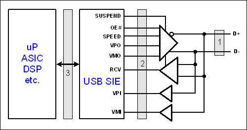
Figure 1. A USB peripheral can be isolated in three positions: position 1, USB bus; position 2, transceiver interface; position 3, application interface. In most designs now, SIE and transceiver are integrated together, and isolation at position 2 cannot be achieved.
The block diagram of USB peripherals is shown in Figure 1. Looking at the diagram from right to left, the USB transceiver is connected to D + and D-, and the transmission or reception of data is controlled by OE (output enable). The intermediate unit is a USB serial interface engine (SIE), whose role is to convert bus signals (sent and received by the transceiver) into byte data or USB signals for use by USB peripherals. The leftmost unit is the application circuit, which may be a microprocessor, an application specific integrated circuit, or a digital signal processor (DSP).
The gray rectangles labeled 1, 2 and 3 show three possible locations for placing the optocoupler and isolating the USB device from the host computer. 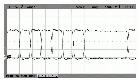
Figure 2. The oscilloscope displays USB D + and D- signals (position 1 in Figure 1). The 83ns bit time and closely matched rise / fall times make it difficult for optocoupler isolation to maintain signal fidelity. D + and D- are bidirectional signals, making isolation more complicated.
Position 1 The following reasons indicate that it is impractical to perform optocoupler isolation on the USB bus, as shown in Figure 2: The signal rate is 12MHz, which is too expensive for a cost-effective isolator. The transmission delay and deviation of the D + and D- signals must be completely consistent, and it is difficult to meet the consistency requirements using optocoupler isolators. The bus is bidirectional, and the isolator is unidirectional, making the optocoupler isolation more complicated. And for a peripheral device using an integrated transceiver, the OE signal (indicating the direction of transmission) cannot be obtained. Position 2 uses a USB peripheral with an external transceiver whose transceiver interface is exposed to the outside, and optocoupler isolation can be considered for these unidirectional signals. Nevertheless, this location has the same problem as location 1: the data rate is too high, and there are multiple 12MHz signals that need to be isolated. The VPO, VMO, RCV, VPI, and VMI signals all run at 12 MHz, and the consistency of transmission delay and deviation of these signals must be strictly maintained. In addition, in modern USB design, SIE and transceiver are integrated on the same chip, it is difficult to obtain this interface.
Position 3 This is the most promising location for isolation. The working speed of this interface is lower than the USB data rate and line rate, and the interface can be composed entirely of unidirectional signals. In fact, an ideal interface should only use a small amount of unidirectional signals, and the data rate of these signals is much lower than the USB 12MHz signal rate.
The ideal interface to meet these requirements is SPI (Serial Peripheral Interface), which is defined by Motorola and is now used in many semiconductor devices. Because of its simplicity and efficiency, SPI has become a very popular interface.
SPI basic signal table 1. SPI signal SPI Signal DescripTIon Comments SS # Slave Select Selects the chip for data transmission, supplied by the master MOSI Master Out Slave In UnidirecTIonal data pin MISO Master In Slave Out UnidirecTIonal data pin SCLK Serial Clock Serial clock, supplied by the master
Table 1 shows the four signals of the SPI interface. SPI is a master-slave interface. The master interface starts and controls communication with a slave interface. The host provides the slave select signal (SS #) and serial clock (SCLK) for synchronous data transmission. The SPI interface has four clock modes, specifically determined by two mode signals CPOL (clock polarity) and CPHA (clock phase). These signals are expressed as (CPOL, CPHA).
Figure 3 describes the SPI data transmission between the microprocessor and the SPI slave device. Figure 3 uses the most common SPI mode (0,0). In the (0,0) mode, the clock is low in the inactive state. The SPI master prepares the MOSI data before the first rising edge of SCLK. The SPI data changes on the falling edge of SCLK, and both the master and slave devices sample the data on the rising edge. 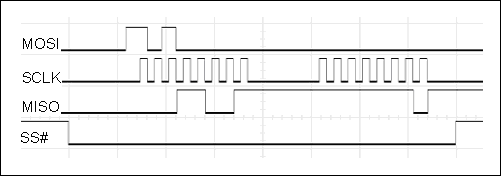
Figure 3. SPI interface working in mode (0,0), if the SCLK signal is active low (quiescent state is high), the same interface can also work in mode (1,1). These low-frequency signals are easily optically isolated.
It is easy to implement an SPI interface on a microprocessor, even a microprocessor without a hardware SPI unit. The SPI interface only requires the microprocessor to construct the signal of Figure 3 through 4 general-purpose IO pins (GPIO), and the subroutine can be realized by directly triggering the read and write operations of the IO pins.
Figure 4 shows the difference in data rate between SPI and USB when the USB peripheral controller uses the SPI interface. In the figure, the main controller implements the USB keyboard function and periodically lights an LED light. The SPI data transmission shown in Figure 5 can be indicated by LED flashing (triggering an output bit); USB communication requests keyboard data for the USB host.
The difference in data rate between the two buses is significant. The lower frequency unidirectional SPI signal is easier to isolate than the 12MHz bidirectional USB bus signal. The SPI signal makes the isolation method very simple, can operate at any frequency, and is suitable for various optical isolators. 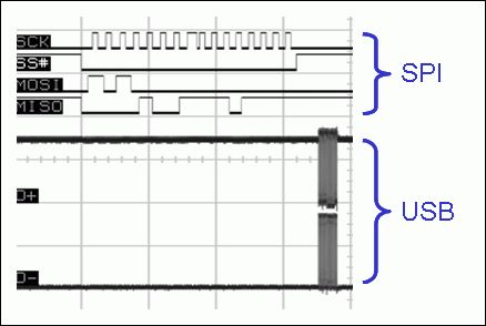
Figure 4. Comparison of SPI data rate and USB signal rate. SPI signals are easier to transmit through optocouplers.
How does the system coordinate the SPI bus rate and USB signal rate of a USB controller with huge differences according to Figure 4? One of the advantages of USB is to achieve "self-throttling" through internal flow control. Signal flow control is accomplished by using the "NAK" (non-reply) handshake signal. Thus, the peripheral device informs the host that the requested data is not ready, and the host should try again later.
SPI data rate and USB NAK 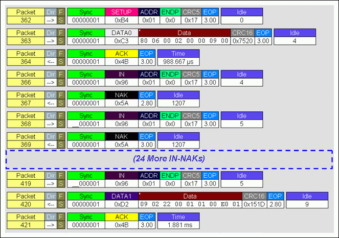
Figure 5. Low-speed peripherals of the USB bus respond to host IN data requests. The host sends a data request in packets 362-364. The peripheral device sends out a packet 420 indicating that the data is ready. The inserted IN-NAK packet is USB flow control, and the peripheral device always responds to NAK before the data is ready.
Figure 5 shows the flow control mechanism of USB data transmission. Starting from packet 362, the host issues a Get_Descriptor-ConfiguraTIon request. The information packet 363 from the second byte to the last byte of 09 means that the host requests the peripheral to send 9 bytes of data. The peripheral device responds to the request in the information packet 364, and then decodes the request, and loads the requested data into the end 0 of the data FIFO. Low-speed peripherals need a certain amount of time to answer this request, and the low-speed SPI bus will further extend the response time.
After 988.667 microseconds (after packet 364), the host starts to request data in packet 366. The peripheral hardware has no data, and the USB hardware automatically generates a NAK handshake response, indicating "busy, try again later." The host retries in packet 368 and gets the same NAK response from the peripheral. This IN-NAK process continues until the information packet 419, the peripheral device finally completes the loading of the requested data, and prepares for data transmission at the end 0 of the data. At this time, the peripheral device replaces the NAK with a 9-byte data packet response in the information packet 420, and the host responds in the information packet 421.
The IN-NAK response (marked with a dotted rectangle in Figure 5) may occur multiple times, which means that there is no minimum limit on the operating rate of the SPI interface. Allows designers to adjust the SPI data rate to suit optocoupler selection in cost-effective designs.
Isolated USB design example 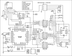
Detailed circuit diagram (PDF, 204kB)
Figure 6. Schematic diagram of an isolated USB design. The left part is powered by the USB bus itself, and the right part is powered by an isolated power supply. The isolation at the SPI interface makes the design simple and is not affected by the timing of the USB bus.
Figure 6 is built using Atmel®'s low-cost microprocessor AtTiny13 (U6), optocoupler HCPL-2531 (U3-5) and MAX3420E (U1), MAX3420E is a USB peripheral controller with SPI interface. Although U6 does not include a hardware SPI unit, the SPI interface can be easily implemented by "bit-wise control" of the GPIO pins. U1 provides four general-purpose input and four general-purpose output pins to replace (add to) U6 to realize SPI interface pins. This design uses two output pins to drive the LED indicators D1 and D2, and one input pin is connected to the button PB1. Because U1 itself contains IO pins controlled by the SPI interface, these IOs are essentially isolated from U6, so no additional isolation is required. 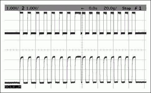
Figure 7. SPI SCLK signal on both sides of the isolated interface, upper part: ISOVCC = 8.3V, ISOGND = 5V. Lower part: powered by USB: VCC = 3.3V, GND = 0V.
Figure 7 shows the SCLK signals on both sides of the isolation interface. The baselines of the two curves are at the bottom of the screen. The upper curve shows the SCLK signal generated by U6, but with a 5V offset. 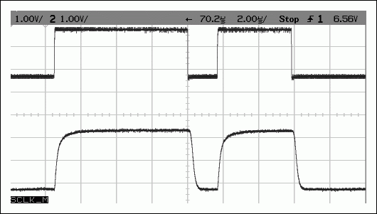
Figure 8. Isolated SCK signal (upper) and SCK signal (lower) on the MAX3420E side, enlarged scale display.
FIG. 8 is an enlarged graph of FIG. 7 for illustrating the performance of the optocoupler. The resistance chosen in this design causes the optocoupler to have a 0.5µs delay at the starting position. The short pulse in the middle of SCLK is generated by the program that U6 drives the SCLK IO pin. This part of U6 program is shown in Figure 9. 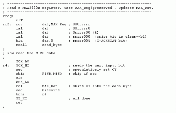
Figure 9. AtTiny13 assembler program to read the MAX3420E register. Here you can adjust the timing of the SPI interface to improve the cost-effectiveness of the optocoupler.
Before the r4 label, the SCK signal is driven low and then driven high again (SCLK_LO and SCLK_HI are assembly macros, and it is easy to assign values ​​to the IO pins of the actual circuit without changing the code).
By inserting a small amount of NOP instructions between these two sentences, the narrow pulse in Fig. 8 can be widened, so that it is possible to use a low-speed optocoupler (which means lower cost). This method demonstrates the flexibility of using the SPI interface in optically isolated applications.
Conclusion Due to the high-speed, bidirectional and strict consistency requirements of USB data signals, the design of electrically isolated USB faces many challenges. If you isolate the interface between the USB controller and the application processor (position 3 in Figure 1), the isolation problem will become simple because the interface can run at any rate. The low signal rate of position 3 makes it ideal for low-cost optocoupler solutions. For any isolation design, the fewer lines that need to be isolated, the lower the cost. Because the SPI interface uses only four low-speed, unidirectional signal lines, the SPI interface is an ideal location for isolation. Because the MAX3420E can communicate with any microprocessor through a simple SPI interface, it is an ideal solution for adding USB functions to embedded systems, and also provides a simple isolation solution for the system. The MAX3421E can also be used as an isolated USB host device. The MAX3421E can be used as a peripheral device or a host device, using the same SPI interface as the MAX3240E.
Abstract: If you must isolate a device connected to a PC, people will naturally choose the USB interface. USB's extensive industrial support and simple structure (USB cable has only 4 lines) make it a universal PC interface. The embedded system with USB controller and SPI interface can easily realize electrical isolation. The SPI interface consists of a simple unidirectional signal line and can be run at any rate.