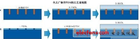
Early IEEE academicians Saraswat, Rief, and Meindl predicted that "chip interconnects may slow down or stop the history of the semiconductor industry...", for the first time, it is proposed to explore the 3D integration technology of circuits. In September 2007, the Semiconductor Industry Association (SIA) declared: "In the next 10-15 years, the ability to shrink transistor size will be limited by physical limits," so the need for 3D integration becomes more apparent. New device structures, such as carbon nanotubes, spintronics or molecular switches, are not ready for 10-15 years. 5 new assembly methods, such as 3D integration technology, have been brought up again. The memory speed lag problem is another driving factor for 3D integration. It is well known that memory access speeds are slower relative to processor speed, causing the processor to be stalled while waiting for memory to acquire data. In multi-core processors, this problem is even more serious and may require direct memory and processor bonding. 3D IC integration technology rescue In February 2005, when ICs Going VerTIcal was published, almost no readers recognized the technological advances that occurred in 3D IC integration. They believed that the technology was just a laminate and wire bond, and it was a back-end packaging technology. Today, 3D integration is defined as a system-level integrated structure in which multi-layer planar devices are stacked and connected in the Z direction via through silicon vias (TSVs) (Figure 1). A number of processes have been developed to make such a laminate structure, and the key technologies listed below are: ■TSV fabrication: Z-axis interconnects are connections that penetrate the substrate (silicon or other semiconductor material) and are electrically isolated from each other. The size of the TSV depends on the data acquisition bandwidth required on a single layer; ■Layer thinning technology: the initial application needs to be thinned to about 75~50μm, and in the future it needs to be thinned to about 25~1μm; ■Alignment and bonding techniques: either between the chip and the wafer (D2W), or between the wafer and the wafer (W2W). By inserting TSVs, thinning and bonding, 3D IC integration eliminates a significant portion of the packaging and interconnect process. However, it is not fully understood at this point that these need to be integrated in the entire manufacturing process. It seems that for the TSV process, it can be obtained through IDM or fab in the IC manufacturing and thinning process, and the bonding can be realized by IDM or by an external semiconductor assembly and test provider (OSATS) in the packaging operation. But this is likely to change as the technology matures. What is likely to happen in the future is that 3D IC integration technology will start when the development route between IC manufacturing and packaging overlaps. 3D process selection TSV can be fabricated in the IC manufacturing process (via first), or after the IC is fabricated (after via). In the former case, the front-end interconnect (FEOL) type TSV was fabricated before the IC wiring process began, and the back-channel interconnect (BEOL) type TSV was implemented in the IC manufacturing process during the metal wiring process. . FEOL-type vias are fabricated on blank silicon wafers before all CMOS processes begin (Figure 2). The conductive material used must be able to withstand the thermal shock of subsequent processes (usually above 1000 ° C), so only polysilicon materials can be used. TSVs fabricated in the BEOL process can use either tungsten or copper, and in general, the fabrication process is early in the overall integrated circuit process to ensure that the TSV does not occupy valuable interconnect routing resources. In both FEOL and BEOL cases, the TSV must be designed into the IC wiring. TSV can also be fabricated after the CMOS device is manufactured. Completed prior to the bonding process or after the bonding process. Since the CMOS device has been fabricated, the wafer does not need to be subjected to high temperature processing even when the via is formed, so a copper conductive material can be used. Obviously, the blank areas in which these vias are made need to be considered when designing the chip. If you can choose, whether it is FEOL or BEOL solution, as long as it is made in the foundry of TSV, it is a relatively simple choice. The BEOL interconnect layer is a complex mixture of different media and metal layers. Etching through these layers is difficult and is determined by different products. Fabrication of TSVs by etching through the BEOL layer after a complete IC fabrication can hinder routing channels, increase routing complexity and increase chip size, and may require an additional wiring layer. Since fabs such as TSMC (Taipei, Taiwan) and Charter (Singapore) have announced that they are interested in vector-based TSV manufacturing, making vias in IC manufacturing processes will be a more viable option.
Our factory have more than 8 years experience in Automotive Wire Harness. We got TS16949 certificate several years ago. Our factory often purchase automotive Connectors from TE, DELPHI, JAE and so on.
We have already got more than 200 kinds of automotive wire harness for our customers and all of them have been not only selling well in mainland China but also exported to Europe, North & South America, Southeast Asia and many other countries and regions. We have relationships with many famous international companies.
Automotive Wire Harness Automotive Wire Harness,Custom Automotive Wire Harness,Automotive Cable Assembly Wiring Harness,Auto Wiring Harness Shareconn Development CO.,LTD , http://www.share-conn.com